

Abstract
We report the temperature and gate-voltage-dependent electrical properties of lead-zirconate-titanate-gated MoS2 field-effect transistors (MoS2-PZT FETs) within a temperature range of 300 to 380 K. The MoS2 transistors with PZT gating exhibit large reproducible clockwise hysteresis, which is induced by the dynamic charge-trapping/de-trapping process of interfacial states between PZT films and MoS2 channels under the modulation of ferroelectric polarization of PZT films. In this way, the modulation of the gate effect on the hysteresis behavior has been achieved by activating the dynamic charge-trapping/de-trapping process in the interfacial states under different Vgs. Moreover, the temperature dependence of the current in the range of 300 to 380 K indicates thermally activated hysteretic behaviors. The hysteresis in the transfer characteristics of MoS2-PZT FETs shows a simultaneous enlargement with increasing temperature, which can be attributed to the thermally sensitive dynamic trapping/de-trapping process of interfacial states.
Export citation and abstract BibTeX RIS
1. Introduction
Two dimensional (2D) materials such as graphene or layered transition metal dichalcogenide (TMDC) materials have received considerable research interest and have become promising advanced semiconductor materials due to their unique properties, such as high charge-carrier mobility [1, 2] and wide applications in electronic devices [3–5]. Compared to graphene, TMDCs are characterized by layered crystal structures with layers composed of strong X-M-X interlayer covalent bonding (where M and X represent transition metal and chalcogen elements, respectively). Among typical TMDCs such as WSe2 [6], MoS2 [7] and WS2 [8] et al MoS2 is one of the most interesting materials with a sandwich structure consisting of covalently bonded S–Mo–S atoms stacked in planes. Unlike the zero-band-gap structure of graphene, MoS2 is an n-type semiconductor with a 1.2 eV indirect band gap of bulk MoS2 to a 1.8 eV direct band gap of single-layer MoS2 [9]. Benefiting from its unique properties, such as large band gaps, satisfactory electron mobility, high current on/off ratio, and good thermal stability [10], MoS2 has been widely used as a functional material in practical electronic device applications, such as thin-film logic circuits and amplifiers with high gain [11, 12]. Aside from this, various research into the transistors based on ferroelectric films have also been reported, such as photodetectors and non-volatile memory devices [13–16]. Recently, MoS2-based field-effect transistors (FETs) have been reported with a ferroelectric polymer P(VDF-TrFE) as top-gate dielectrics and single- to triple-layered MoS2 nanosheets as a channel layer for non-volatile memory applications [17]. The combination with MoS2 and ferroelectric films indicates a potential route toward non-volatile 2D metal dichalcogenide conduction-channel transistors. Among various ferroelectric materials, the studies of lead-zirconate-titanate-based FETs (PZT FETs) have attracted much attention due to its high remnant polarization, low coercive voltage, good chemical stability and compatibility with microelectronics processes. In our previous work, back-gate MoS2-FETs controlled by PZT ferroelectric gating were prepared and the reproducible hysteresis and non-volatile memory behaviors with high stability were demonstrated [18]. It is interesting, however, that the clockwise hysteresis behavior, which is opposite to the ferroelectric polarization direction, has been widely found in PZT-gating FETs. The origin of this unexpected large clockwise behavior by PZT gating has attracted widespread attention, especially in non-volatile memory applications. Recently, Zhou et al reported a high-performance field-effect transistor-based CVD MoS2 and PZT gate dielectric with small hysteresis, indicating that oxygen vacancies induce the clockwise hysteresis [19]. Additionally, Lipatov et al have demonstrated that the interplay of polarization and interfacial phenomena strongly affects the electronic behavior and memory characteristics of lead-zirconate-titanate-gated MoS2 field-effect transistors (MoS2-PZT FETs) [20]. The interface traps between the atomic-level-thick semiconductor and the substrate are a common problem for 2D-based electronics and have a great impact on their electrical performances [21, 22]. These interface traps may originate from the transfer process of 2D layered materials to the substrate or the atomic-level roughness of the substrate. Based on this, the temperature-dependent transport and hysteresis behaviors of MoS2-FETs with PZT gating have been investigated in order to analyze the dynamic process of interfacial states between MoS2 and PZT, which has not been reported elsewhere.
Therefore, in this paper, we report the temperature (T) and gate voltage (Vgs)-dependent electrical properties of MoS2-PZT FETs. The origin of clockwise hysteresis behaviors opposite to the ferroelectric polarization has been investigated and the back-gate modulation effect on hysteresis has been demonstrated under different sweeping gate voltage at the same temperature. The temperature-dependent hysteresis behaviors with varying T have been studied under different gate-voltage sweeping ranges. The temperature dependence of the electrical performance of MoS2-PZT FETs has contributed to the temperature-sensitive dynamic trapping/ de-trapping process of the interfacial states. The corresponding changes in the max drain current and threshold voltage are observed with varying Vgs and T, which demonstrates such MoS2-PZT FETs remain functional at least as high as 380 K.
2. Methods
2.1. Device fabrication
The MoS2 flakes were mechanically exfoliated from a bulk ingot (SPI Supplies) and transferred onto the PZT/Pt/Ti/SiO2/Si substrates with a 260 nm-thick Pb(Zr0.4Ti0.6)O3 (PZT) layer prepared by a sol-gel process. The Pt layer underneath the PZT films served as the gate electrode, while the PZT films served as the gate dielectric. After the transfer of the MoS2 flakes, electron-beam lithography was used to pattern source/drain contacts, followed by electron-beam evaporation of 20/50 nm Cr/Au electrodes and a lift-off process. A schematic of the MoS2-PZT FET devices is shown in figure 1(a). An optical microscope image of the MoS2-PZT FET devices is shown in the inset of figure 1(b) with the channel length L ∼ 200 nm and width W ∼ 30 μm and the width of the contact bars is about 2 μm.
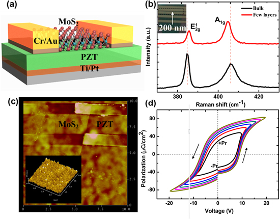
Figure 1. (a) Schematic of MoS2-PZT FET devices with MoS2 flakes as a channel layer and PZT film as bottom -gate insulators. (b) Raman spectra of a few-layered MoS2 sample. The black line represents the bulk MoS2 samples and the red line represents the few-layered MoS2 samples. The inset is the optical microscope image of the fabricated MoS2-PZT FET devices with channel length L ∼ 200 nm and width W ∼ 30 μm and the width of the contact bars about 2 μm. (c) AFM image of MoS2-PZT FET. The inset is the AFM image of PZT films. (d) The polarization–voltage (P–V) characteristics of a ferroelectric capacitor (Au/PZT/Ti/Pt) structure.
Download figure:
Standard image High-resolution image2.2. Characterization
Raman spectroscopy using a wavelength of 532 nm (RM-1000, Renishaw) was used to confirm the MoS2 sheet with few layers. In order to verify the thickness of this MoS2 sheet, the microstructure and morphology of the MoS2-PZT FETs were observed by atomic force microscopy (AFM, SPA 500, Seiko Instruments Inc.) with taping mode. The polarization–voltage (P–V) characteristics were measured by using a ferroelectric test system (Multiferroics, Radiant Company) with a temperature increasing from 300 to 380 K. The temperature-dependent electrical measurements of the device were conducted by an Agilent B1500A semiconductor parameter analyzer with a variable temperature probe station. The test temperature ranged from 300 to 380 K in our experiments.
3. Results and discussion
Figure 1(b) shows the Raman spectra of the typical MoS2 samples. Two typical modes, which are attributed to the in-plane  and out-of-plane A1g vibration, are observed in both few-layered (red line) and bulk MoS2 (black line). The spectrum reveals that the frequency of
  mode increases while that of A1g mode decreases from bulk MoS2 to the exfoliated MoS2 sample, confirming the sample to be about a few layers. An AFM measurement, as shown in figure 1(c), has been conducted to verify the thickness of this MoS2 sample to be ∼2.8 nm, corresponding to the quality of four layers [23]. According to the AFM image of PZT film, as shown in the inset of figure 1(c), the average roughness of PZT films is 0.8995 nm, indicating a dense and uniform surface of the PZT films deposited by sol-gel method. Figure 1(d) depicts the polarization–voltage (P–V) characteristics of a ferroelectric capacitor (Au/PZT/Ti/Pt) structure under different sweeping voltages. It can be seen that our prepared PZT films show a large remnant polarization (2Pr) of about 112.05 μC cm−2 and a coercive voltage of 8 V, which may be due to a good crystal structure or the contribution of conductivity [24, 25].
3.1. The hysteresis behaviors observed in MoS2-PZT FETs with increasing temperature
The basic electrical properties of such PZT-gated MoS2 FETs have been reported in our previous published work [18]. In this paper, we further investigated the electrical performances of the MoS2-PZT FETs with varying max-gate sweeping voltage (Vgmax) under different temperature (T). Figure 2 presents the Ids–Vgs curves of the device under Vgmax of 4, 6, 8 and 10 V, respectively, with temperature ranging from 300 to 380 K. Each cyclic voltage sweeping from −Vgmax to Vgmax to −Vgmax is repeated and the resultant Ids–Vgs loops show good reproducibility under different Vgmax. It is noted that the observed clockwise current hysteresis behaviors are opposite to the expected anticlockwise hysteresis behaviors arising from the polarization effects of the ferroelectric gate dielectric. The origin of the clockwise hysteresis behaviors can be attributed to the dynamic charge-trapping/de-trapping process in the interfacial states between MoS2 and PZT films under the modulation of ferroelectric polarization. On one hand, as a typical oxide ferroelectric material, polycrystalline PZT is usually oxygen-deficient [26]. In the region near the interface between MoS2 and PZT, there are more oxygen deficiencies than in the bulk. On the other hand, the oxygen/water molecules in the ambient absorbed on the surface of PZT films before MoS2 exfoliated on it also contribute to the defects in the interfacial layer. Moreover, some ionic impurities could be introduced during the solution preparation process of PZT films, which also accounted for the defects in the interfacial states. These defects include oxygen deficiencies, the oxygen/water molecules and ionic impurities bounded at on the surface of PZT films could act as electron traps which can dynamically respond to the change of ferroelectric polarization-induced built-in field under different Vgs. As shown in figure 1(d), the applied gate voltage Vgs induces an arrangement of dipoles in the PZT films, which causes a built-in electric field due to the polarization effect. The polarization slightly decreases to the remnant polarization Pr when Vgs is swept from a negative voltage to zero, which induces a large and stable electrostatic field through the interfacial layer between MoS2 and PZT films. The electrons trapped in the interfacial states will obtain sufficiently large energy from the polarization field and be released into the MoS2 channel under the downward ferroelectric polarization field, which results in a dramatic increase of drain current (as shown in figure 2).

Figure 2. (a) The Ids–Vgs curves of MoS2-PZT FETs under different temperatures rising from 300 to 380 K and Vgmax at 4 V (a), 6 V (b), 8 V (c) and 10 V (d), respectively.
Download figure:
Standard image High-resolution image3.2. Analysis of the clockwise hysteresis behaviors induced by the charge-trapping/de-trapping process under ferroelectric polarization
It can be seen from figure 3, that when Vgs sweeps from -Vgmax to 0 V, the electrons already trapped in the interfacial states can be released into the MoS2 channel under the electrostatic field induced by downward polarization, which presents a de-trapping process. These de-trapped electrons moving into the n-type MoS2 channel result in an n-doping effect. As shown in figure 3(a), before the Vgs reaches zero, the polarization intensity decreases slightly, which results in a stable built-in electric field. This stable polarization could build up a stable polarization filed, which would provide the dynamic charges with larger kinetic energy and drive more electrons into the MoS2 channel. This indicates the accumulation of electrons in the MoS2 channel and the dramatic increase in drain current, as shown in figure 2. When Vgs sweeps from 0 V to Vgmax, the polarization of PZT films decreases and is reversed to upward polarization, as shown in figure 3(b). During this process, the built-in ferroelectric field is reduced and the number of de-trapped electrons becomes less, which contributes to a balanced state between the charge-trapping and de-trapping process and indicates a saturated current. Once Vgs sweeps from Vgmax to 0 V, the electrons will be trapped again in the interfacial layer, which results in a drastic reduction of current, as shown in figure 3(c). And when Vgs sweeps from 0 to -Vgmax, the polarization can be reduced and the number of trapped electrons become less, as shown in figure 3(d). Therefore, the current of the n-type MoS2 channel becomes small, representing the OFF state of MoS2-PZT FETs. Above all, the dynamic charge-trapping/de-trapping process of interfacial states between PZT films and MoS2 under the polarization effect of PZT films contributes to the reproducible clockwise hysteresis behaviors. As Vgmax increases from 4 to 10 V, the polarization of PZT films improves, inducing a faster trapping/de-trapping process and enlarged hysteresis behavior, as shown in figure 2. In this way, the modulation of gate voltage in the transport characteristics of MoS2-PZT FETs has been achieved.
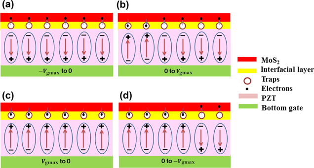
Figure 3. (a) The dominant charge de-trapping process with the Vgs sweeping from −Vgmax to 0 V. (b) The balanced state between the charge-trapping and de-trapping process with the Vgs sweeping from 0 to Vgmax. (c) The dominant charge-trapping process with the Vgs sweeping from Vgmax to 0 V. (d) The balanced state between the charge-trapping and de-trapping process with the Vgs sweeping from 0 to −Vgmax.
Download figure:
Standard image High-resolution image3.3. Temperature-dependent electrical performance of MoS2-PZT FETs
It can also be found that with Vgmax values changing from 4 to 10 V, all the transfer curves exhibit the same change trends with varying T. It can be seen that the size of the hysteresis loop increases with the increasing T. In order to further study the influence of T on the electrical properties of MoS2-PZT FETs, the max currents obtained at polarized saturation states when Vgs swept from -Vgmax to Vgmax are defined as the max drain current. The difference in Vgs that occurs at the current value corresponding to the midpoint of the maximum and minimum possible current values of the device is defined as the memory window (ΔVM) as shown in figure 4(a). The max drain current is calculated from the transfer characteristics of MoS2-PZT FETs as a function of the Vgmax and T in figure 4(b). It can be seen that the max drain current is 2.1 μA at 300 K when the Vgmax is 10 V. With the temperature rising to 380 K, the max drain current increases to 7.3 μA and similar behaviors can be found with Vgmax ranging from 4 to 10 V. The threshold voltage VT is extracted from the onset of significant drain current conduction in the drain current transfer curves, as shown in figure 4(a). In the meantime, the threshold voltages with varying Vgmax and T follow the expected trend for an n-type semiconductor in figure 4(c). The threshold voltages from −Vgs to Vgs under different Vgmax follow in the same way to decrease to more negative values with the increase of temperature. We also extract the memory windows ΔVM from the transfer curves for MoS2-PZT FETs with varying temperature and Vgmax from 4 to 10 V, as shown in figure 4(d). It can be seen that the ΔVM changes slightly with the increase of T under different Vgmax. The possible factors on the temperature-dependent electrical performances of MoS2-PZT FETs may be the polarization of PZT films, the carrier transport characteristics in the MoS2 channel, the change of contact resistances and the interfacial states between PZT and MoS2. In order to find out the crucial factor, the related temperature-dependent measurements have been conducted and discussed below.
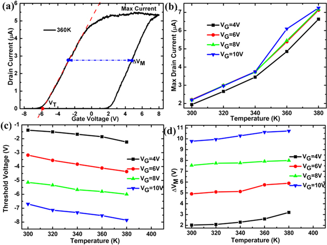
Figure 4. (a) The hysteresis loop of the MoS2-PZT FET device at the Vgmax = 10 V labeling the max drain current, memory window and the threshold voltage. (b) The plots of max drain current versus temperature under different Vgmax of 4, 6, 8 and 10 V. (c) The plots of threshold voltage versus temperature under different Vgmax of 4, 6, 8 and 10 V. (d) The plots of memory window versus temperature under different Vgmax of 4, 6, 8 and 10 V.
Download figure:
Standard image High-resolution imageIn order to gain insight into the dependence of ferroelectric polarization on T, the P–V characteristics with T ranging from 300 to 380 K have been investigated, as shown in figure 5(a). As ferroelectrics, the pyroelectric coefficients of PZT films can be determined by the varying T, resulting in temperature-dependent polarization states. From figure 5(b), the remnant polarization (2Pr) has been plotted as a function of T, indicating that increasing T leads to a weakened polarization of PZT films. It is obviously the case that as the polarization becomes weakened, the current hysteresis loop induced by interfacial charge trapping/de-trapping under the polarization will be reduced (as discussed above). However, as shown in figure 2, it is opposite to the change of the polarization of PZT films with increasing T, which demonstrates that there are other temperature-dependent factors playing a major role. As a FET structure with a two 2-terminal (S/D) device configuration, the temperature dependence of contact resistances between S/D electrodes and the MoS2 channel has been calculated from the output characteristics, with Vgs ranging from 0 to 8 V and T increasing from 300 to 380 K in PZT back-gated FETs with different channel lengths. The results show a slight change with the increase of temperature, as shown in figure 5(c), indicating that the thermally sensitive hysteresis behaviors do not originate from the change of contact resistances with the increasing T. Considering the dependence of carrier transport characteristics in the MoS2 channel, the scattering mechanism has been found to be a critical factor. It has been reported that at temperatures below 100 K, temperature-independent mobility is limited by Coulomb scattering, whereas, at temperatures above 100 K, phonon-limited mobility decreases as a power law with increasing temperature [27]. Therefore, the current of MoS2 should be reduced with the enhancement of phonon scattering when T increases from 300 to 380 K. However, this also goes against the observed temperature-dependent transport curves, as shown in figures 2 and 4. Therefore, it can be inferred that the temperature dependence of the interfacial states contributes to the enlargement of transport and hysteresis behaviors of MoS2-PZT FETs. At the negative gate voltage, the charge de-trapping process will become more drastic to release more electrons to the MoS2 channel at a faster speed with the increase of T, which results in a larger drain current and a more negative threshold voltage, as shown in figure 4. The process of electrons trapped again in the interfacial layer will also be enhanced with the increase of T, inducing a dramatic decline of drain current. Therefore, sets of transfer characteristics with different Vgmax have a similar dependence on temperature.
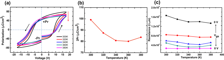
Figure 5. (a) The polarization versus voltage (P–V) characteristics of the ferroelectric capacitor (Au/PZT/Ti/Pt) structure with T ranging from 300 to 380 K at a frequency at 10 KHz. (b) The remnant polarization (2Pr) calculated from figure 5(a) has been plotted as a function of T. (c) The temperature dependence of the contact resistances between S/D electrodes and the MoS2 channel with the Vgs ranging from 0 to 8 V at a step of 2 V.
Download figure:
Standard image High-resolution imageFigure 6(a) shows the semilog plot of the transfer characteristics with gate voltage sweeping from −10 to 10 V and the temperature ranging from 300 to 380 K. The on current reaches 2.2 μA at T = 300 K and the corresponding current Ion/Ioff ratio is over 104. While for a temperature of 380 K, the on current is 7.3 μA at Vgs = 10 V and the corresponding current Ion/Ioff ratio is over 103. The Ion/Ioff ratio shows a minor decrease as the temperature increases, while the total change of Ion/Ioff ratio remains within 1 order of magnitude, as shown in figure 6(b). In the n-type MoS2, the minority carriers (holes) have more sensitive temperature dependence than electrons. When Vgs is swept from positive to negative, the electrons trapping/de-trapping into/out of the interfacial states activated by increasing temperature become more dynamic, resulting in an increasing Ioff and a decreasing Ion/Ioff. Moreover, the output characteristics (drain-source current Ids versus drain-source voltage Vds) and their temperature dependence have also been investigated. The output characteristics (Ids−Vds) with Vgs ranging from 0 to 8 V at a step of 2 V at 300 K are shown in figure 6(c). Here, the curves show well-defined linear regimes at low biases and have a tendency toward saturation at high biases, indicating the typical pinch-off characteristics of n-type semiconductor FETs. Figure 6(d) shows the temperature dependence of the output characteristics with Vgs at 2 V and T increasing from 300 to 380 K, which indicates an increase of drain current due to the enhanced dynamic process of charge trapping/de-trapping with the increasing temperature.

Figure 6. (a) Semilog plots of the transfer characteristics of MoS2-PZT FETs with T varying from 300 to 380 K and Vgs swept from −10 to 10 V. (b) The plots of Ion/Ioff ratio versus temperature under different Vgmax of 4, 6, 8 and 10 V. (c) The output characteristics (Ids-Vds) of MoS2-PZT FETs with Vgs ranging from 0 to 8 V at a 2 V step. (d) The temperature-dependent output characteristics of such a structure with Vgs = 2 V and the temperature increasing from 300 to 380 K.
Download figure:
Standard image High-resolution image
4. Conclusions
In conclusion, MoS2-PZT FETs have been fabricated and their temperature and Vgs-dependent hysteresis behaviors of MoS2-PZT FETs are carefully investigated. The clockwise hysteresis behaviors of MoS2-PZT FETs have been demonstrated to be induced by the dynamic charge-trapping/de-trapping processes of the interfacial defect states under the modulation of the ferroelectric polarization of PZT films. The gate effect on electrical performances of MoS2-PZT FETs has been found to be achieved by modulating the polarized states of PZT films, which further induces the dynamic charge-trapping/de-trapping processes. With the increase of temperature, the max drain current shows a great increase and the threshold voltage becomes more negative. These temperature-dependent electrical performances are ascribed to the temperature-sensitive characteristics of interfacial states, which stimulate more drastic charge-trapping/de-trapping processes. The memory window shows little increase and the change of Ion/Ioff ratio remains within one order of magnitude with the temperature varying from 300 to 380 K. Overall, these results reveal the origin of clockwise hysteresis in the MoS2 channel by PZT gating and help guide future efforts to realize high-performance MoS2-PZT FETs for electronic device applications.
Acknowledgments
The authors are grateful for the financial support from the National Natural Science Foundation of China (51372130, 51672154), and the Open Research Fund Program of the State Key Laboratory of Low-Dimensional Quantum Physics (No. KF201517).