
Abstract
We present an atomistically informed parametrization of a phase-field model for describing the anisotropic mobility of liquid–solid interfaces in silicon. The model is derived from a consistent set of atomistic data and thus allows to directly link molecular dynamics and phase field simulations. Expressions for the free energy density, the interfacial energy and the temperature and orientation dependent interface mobility are systematically fitted to data from molecular dynamics simulations based on the Stillinger–Weber interatomic potential. The temperature-dependent interface velocity follows a Vogel–Fulcher type behavior and allows to properly account for the dynamics in the undercooled melt.
Export citation and abstract BibTeX RIS

Original content from this work may be used under the terms of the Creative Commons Attribution 3.0 licence. Any further distribution of this work must maintain attribution to the author(s) and the title of the work, journal citation and DOI.
1. Introduction
The growth of silicon is relevant for a wide range of technological processes in semiconductor industry, including the production of polycrystalline silicon for photovoltaics by electromagnetic casting, edge-defined film feed methods, ingot directional solidification techniques, and also liquid phase crystallization. Currently, over 90% of the commercial solar cells are made from single- or multi-crystalline silicon. The production volume of solar cells using the multi-crystalline silicon is higher than that of single-crystalline silicon. In order to obtain a detailed understanding of the interplay of process parameters and the resulting microstructure, computer simulations have become an increasingly important tool. However, modeling of nucleation processes and growth morphologies requires a quantitatively correct description of anisotropic interface energies and mobilities of the crystal-melt interface.
Simulations of the solidification of multi-crystalline Si including the evolution of grains can be divided in macroscopic, microscopic and atomistic methods. On the macroscopic scale, cellular automata and geometric models were proposed, which are most efficient, but lack some physical details. Atomistic molecular dynamics simulations have been successfully applied to simulate solidification of silicon and thus offer a route for revealing details of the growth kinetics [8, 9, 36]. Because of the enormous computational effort, however, these models are restricted to relatively small system sizes of typically not more than a couple of million atoms. This is why for modeling phenomena on the microscopic scale, phase field models (PFM) have emerged as a promising and powerful tool for simulating free boundary problems with complex morphological evolution. Since the transport equations for heat and mass and the phase field are solved simultaneously, the effects of surface tension, nonequilibrium, and anisotropy can be directly included. PF models are based on physical parameters and can take into account anisotropies of interface energies and mobilities.
In the context of silicon grain growth PFM face, however, several challenges. The large anisotropy of interface energies and directional dependent mobilities determine in a delicate way the combination of occurring facets. Moreover, the solidification process is in general much slower than for metallic systems and thus there is smaller thermal gradients. A technical drawback of PFM lies in the fact that the minimum mesh size has to be smaller than the interface thickness, while a realistic interface thickness is only on the order of the capillary length approximately several Ångstrom. The large body of literature on phase-field models for transitions between liquid and solid phases has been reviewed, for example in Boettinger et al [5], Wheeler et al [46] and more recently in Moelans et al [32] and in the context of solidification and dendritic growth by Steinbach [40]. Especially, for the problem of excimer laser annealing of a  layer on an amorphous substrate Magna et al [30] and Shih et al [39] developed specific phase-field models based on coupled equations describing the thermal, phase and impurity redistribution during the annealing process. A recent review on liquid thermal annealing was published by Fisicaro et al [15]. However, in the PFM existing studies dealing with silicon mostly qualitative assumptions on free energy densities, anisotropic interface energies and mobilities were used. On the other hand, detailed information on melting points, interface velocity and formation of defects during crystal growth are in principle available from molecular dynamics simulations and can directly be used. Therefore, it seems natural to ask if both modeling approaches can be combined to yield quantitative accurate models, that are amenable to large scale simulations. This has been the concern of a number of studies in recent years, where it has been shown how atomistic molecular dynamics computations can be used to obtain quantitative information for kinetic and thermodynamic properties to correctly predict the dynamics of the corresponding multi-phase systems using phase-field models. In the context of dendritic solidification, for example, Hoyt et al [21] developed a method for extracting anisotropic interface energies from atomistic molecular dynamics simulations and used them in in a phase-field description with weak anisotropy of the solid–liquid interface. Similarly, Bragard et al [6], derived PF-parameters for predicting the dendrite growth velocity as a function of undercooling in pure
  . A more detailed overview on these problems can be found in Hoyt et al [22]. For the solidification of the alloy systems of
  , Danilov et al [10] and Guerdane et al [20] addressed the more fundamental question if molecular dynamics simulations and the phase-field approach can give quantitative equivalent results. At least for these specific alloy systems they found good agreement in quantities such as the melting rates by comparing their numerical results.
Interestingly, there is no published study in which the thermodynamic parameters of a phase-field model for solidification of silicon are extracted from atomistic simulations, although some relevant data are available [4, 7, 13, 19]. Thus, the focus of this study is to establish a phase-field model, where the complete set of necessary parameters is derived from molecular dynamics simulations based on the Stillinger–Weber (SW) interatomic potential for  [42]. In particular, we incorporate a consistent description of the Vogel–Fulcher-type temperature dependence of the interface velocity of
  [18, 41, 44]. In order to establish the necessary phase-field parameters we investigate three distinct planar interface orientations.
2. From an atomistic to a phase-field description
In the diffuse interface description the transition between a liquid and crystalline phase is introduced by a phase-field variable  . It is a function in space and time that varies from
  in the liquid state to
  in the crystalline state. In the simplest setting for a pure melt in the isothermal case a free energy functional

can be derived from thermodynamic considerations [5]. The bulk free energy density  is a function of the phase-field variable and temperature. The gradient energy coefficient σ is related to the steepness or width of the transition from the liquid to the solid phase. For anisotropic interfacial energies, this also depends on the orientation angle normal to the contours of constant p as shown in [26, 31]. Since we consider a one-dimensional model, different σ parameters are chosen depending on the given interface orientation
  , denoted by
  . Upon minimization of the decreasing free energy functional
  the evolution equation for
  is obtained as

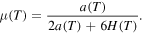
where  denotes the interfacial mobility parameter of the phase field describing the relaxation dynamics of the interface. The mobility parameter
  depends on temperature and also on interface orientation.
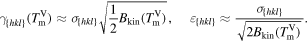
As schematically sketched in figure 1, the free energy density F is convenientally chosen as double-well potential with minima at p = 0 for the liquid and p = 1 for the crystalline phase and with a maximum in between. We choose a fourth order polynomial in p with temperature dependent coefficients. The temperature dependent minima correspond to the free energies of the liquid and solid phase and can be calculated from atomistic simulations by thermodynamic integration (see section 3.2).
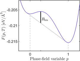
Figure 1. Example of the bulk free energy density F and its kinetic barrier Bkin at temperature  (less than TmV). Bkin is the kinetic barrier, that has to be overcomed to pass from one phase into the other.
Download figure:
Standard image High-resolution imageBy measuring the normal velocity

of a moving flat interface in a molecular dynamics simulation (see section 3.4) one can directly determine the orientation dependent mobility M of a solid–liquid interface. The driving force F is determined by the free energy difference of the liquid and solid phase at a given temperature and can be independently calculated. However, the thermodynamic mobility M obtained in such a manner, cannot be used as parameter in a phase-field model. The reason is that in a phase-field simulation the system has to overcome the barrier Bkin dividing the two potential wells of the free energy density F as sketched in figure 1. As we show in section 4.1 in equations (11) and (14), the kinetic barrier Bkin has a direct effect on the free energy density. This contributes to the mobility of the phase-field and thus MPF cannot be identical to M. This is often disregarded in parametrizations for recrystallization phenomena as e.g. in [15, 39, 46].
The second term of the integrand in equation (1) describes the crystal-melt interfacial energy, which scales with the coefficient  . For a given interfacial energy
  , which can again be obtained from molecular dynamics simulations, and a fixed interface width
  , one can adjust Bkin and
  . The relations between
  and
and  are
are
as given in [1].
Again, it should be noted that the parameter σ is often considered as freely adjustable. Thus, for a given interface energy, rescaling the σ parameter for numerical reasons is equivalent to rescaling of the interface width, which in turn means that the parameter Bkin needs to be readjusted, if the interface energy shall remain unaffected.
In this paper, we choose  as a physical parameter describing the width of the interface for the
  growth plane and use interface velocities, interfacial energies and free energy densities obtained from molecular dynamics simulations.
The velocity versus temperature relationship is fitted to an equation describing the competition between kinetics and thermodynamics of the crystallization process. In section 4.3, the remaining parameter of the phase-field model, the mobility  , is then obtained by a shooting method applied to (2) in one dimension, such that the crystallization velocity of the phase-field simulation agrees with the growth velocity calculated by means of molecular dynamics, which we prove numerically in section 4.4.
3. Atomistic model and parameter calculation
3.1. Method
Molecular dynamic calculations are performed using the SW interatomic potential for silicon [42], which describes the structure of the molten phase realistically, and reproduces the experimental melting point [25, 28, 29, 38]. We calculate thermal properties and interfacial velocities with the widely used LAMMPS code [35] and obtain free energy densities via using the MD++ code [37]. In table 1 we present a summary of the thermal properties obtained using the SW potential along with results form previous simulations and experiments.
Table 1. Heat capacity, latent heat and melting point of silicon. TmMD is the melting point obtained from moving interface simulations, TmV is the melting point obtained at constant volume from the adiabatic switching method (see section 3.2).

|

|
 (kJ mol−1) (kJ mol−1) |
TmMD(K) | TmV(K) | |
|---|---|---|---|---|---|
| (J mol−1 K−1) | (J mol−1 K−1) | ||||
| SW-pot. | 26.9 | 28.7 | 31.7 | 1683 | 1697.12 |
| other sim. | 30.9 [7] | 1682 [17] | |||
| Exp. | 26–29 [12] | 27.2 ± 1.5 [12] | 50.25 ± 0.6[12] | 1683[42] | |
| Data | (900–1687 K) | ||||
We initialize a simulation box containing 4096 atoms in the diamond structure and heat it up. For doing so, we apply a Nosé–Hoover thermostat with a rate of 1013 K s−1. After melting occurs, we cool it down with the same rate and calculated the specific heat and latent heat from the average total energy. Clearly, the specific heat and melting point are in good agreement with the experimental finding. The latent heat, in contrast, is low compared to experimental measurements. The reason is that we describe the solid phase and the liquid phase by a single empirical model despite their different bonding mechanisms [37]. The melting point TmMD calculated from a simulation cell with solid–liquid phases co-existence is almost exact compared to the experimental value of 1683 K and in good agreement with earlier simulations [14, 17]. If the intersect of free energies calculated by the adiabatic switching method at constant volume is used (see section 3.2) the calculated melting point  is slightly higher. In order to be consistent with the free energy data, we use TmV as melting temperature for the phase-field model.
3.2. Free energy densities
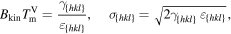
For calculating the free energy density, we use a supercell with 512 atoms and periodic boundary conditions in all three directions. The actual calculation of the free energy is performed using both adiabatic switching and reverse scaling [11, 45] as implemented in the MD++ software package by Ryu and Cai [37]. In order to be consistent with our phase-field model, we modify the code such that an NVT ensemble is used, the initial volume for both phases—solid and liquid—is equal to the equilibrium volume of the crystalline silicon supercell at 0 K. The free energy density is calculated then by dividing the obtained free energies by that same volume. Furthermore, in our approach we include the free energies of the amorphous state calculated by Broughton and Li [7]. The results are presented in figure 2. The melting point used in the phase-field model is the one obtained from this free energy calculation,  , which is the temperature at which the amorphous/liquid and solid free energies intersect. We point out that this value does not correspond to the experimental value or to the values obtained from direct interface calculations (see table 1). The reasons for this discrepancy are the NVT ensemble we used for the free energy calculation and a numerical error in the adiabatic switching and reverse scaling methods, used for a large temperature intervals like the one we analyze.
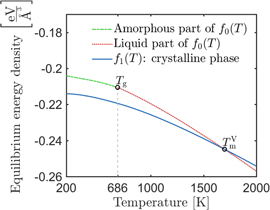
Figure 2. Minimum values for the free energy density for liquid/amorphous ( ) and crystalline (
 ) equilibrium to the SW potential for a temperature range of 200–2000 K. The free energy equilibrium values are calculated with the codes provided by Ruy and Cai [37]. For the liquid branch, Tg points out the glass transition. The free energies for the amorphous phase were calculated by Broughton and Li [7].
Download figure:
Standard image High-resolution image3.3. Interfacial free energies
Interfacial free energies calculated with the SW potential are available in literature from Apte and Zeng [2], who used molecular dynamics to determine  and
and  at the melting point. Their mean values are given in table 2. The most densily packed
  orientation has the lowest interface energy, while the (110) direction exhibits nearly the same excess energy. This is obviously at odds with the equilibrium shape of Si grains embedded in a melt, which show a Wulff shape with (111) and (100) facets only. Thus,
  is obviously underestimated by the SW-potential. Since the purpose of this study is to devise model parameter, which allows us to directly combine phase-field and molecular dynamics simulations with consistent model parameters corresponding to the SW potential, we adopt these values for our parametrization.
Table 2. The crystal-melt interface free energies γ at the melting point TmV for the orientations {100}, {110} and {111} calculated by Apte and Zeng in [2].
| Orientation | {100} | {110} | {111} |
|---|---|---|---|
 in eV Å−2 in eV Å−2 |
0.026 | 0.0218 | 0.0212 |
3.4. Interface velocities
We calculate interface velocities from molecular dynamics simulations of moving planar liquid–solid interfaces with different crystallographic orientations at constant temperature ![$T\in [800,2000\,{\rm{K}}]$](https://content.cld.iop.org/journals/0965-0393/25/6/065015/revision2/msmsaa7862ieqn37.gif) . For this, we initialize a simulation box of about 43 × 43 × 130 Å, like the one shown in the left-hand side of figure 3. Such box contains 12 000–13 000 atoms, depending on the crystal orientation and has periodic boundary conditions in all three directions. The box sizes in x- and y-direction are adjusted in order to obtain a single crystal without lattice defects near the boundaries of the box. We start our simulation with an equilibration phase using a Nosé–Hoover thermo- and barostat for 10 ps at the desired temperature in order to consider thermal expansion of the box. One timestep corresponds to 1 fs. The box dimensions are left free to vary independently of each other. For the case of temperatures below the melting point, as shown in the left-hand side of figure 3, the crystalline part of the box (about
. For this, we initialize a simulation box of about 43 × 43 × 130 Å, like the one shown in the left-hand side of figure 3. Such box contains 12 000–13 000 atoms, depending on the crystal orientation and has periodic boundary conditions in all three directions. The box sizes in x- and y-direction are adjusted in order to obtain a single crystal without lattice defects near the boundaries of the box. We start our simulation with an equilibration phase using a Nosé–Hoover thermo- and barostat for 10 ps at the desired temperature in order to consider thermal expansion of the box. One timestep corresponds to 1 fs. The box dimensions are left free to vary independently of each other. For the case of temperatures below the melting point, as shown in the left-hand side of figure 3, the crystalline part of the box (about  ) is equilibrated at the desired temperature. The remaining atoms are melted at 1000 K above the melting point and then cooled to a temperature near TmMD. While melting, the box dimensions in x- and y-direction are fixed, but in z-direction the box is allowed to shrink or expand. Finally, we run the crystallization for some nanoseconds with a global thermostat at the desired temperature. The x- and y-dimensions are fixed again, but not in the growth direction. For the case of temperatures above the melting point the procedure is analogous. In this case, the lower part of the box (about
  ) is heated up to the desired temperature and, therefore, is melted, while the upper part of the box is kept crystalline with a temperature near TmMD. Then, for some nanoseconds, the complete simulation box is connected to global thermostat at the desired temperature above TmMD.
Figure 3. The schematic of the simulation box used to calculate the interface velocities is presented in the left figure. For temperatures below the melting point the yellow region corresponds to the crystalline silicon and the blue region to the melt. In the case of temperatures above the melting point, the color code is reversed. In the right figure we show the dependence of the average centrosymmetry parameter of melt and solid on temperature. The mean value CScrit(T) is used to determine the position of the crystallization front.
Download figure:
Standard image High-resolution imageTo extract the velocity of the interface, one first has to determine its position at each timestep. There are numerous ways to do so (see [28]), for instance, by monitoring the particle density or the atomic potential energy. The observed parameter only has to fulfill the condition that it is sufficiently different in the solid and liquid phase. In this study, we choose the centrosymmetry parameter [24], which can be calculated for each atom within LAMMPS. It is zero for an atom in a perfect lattice, and gives a positive value for disturbed atomic environments. The average of the centrosymmetry parameter over one atomic layer perpendicular to the growth direction (corresponding to some hundreds atoms) results in a centrosymmetry of 8.5–11 for a liquid layer and 12–13.5 for a crystalline layer. We find that the centrosymmetry of melt and crystal is dependent on temperature, as shown in the right-hand of figure 3.
Therefore, we take the mean value of the centrosymmetry of crystal and liquid as the critical value CScrit in order to distinguish liquid and solid atoms. Using the centrosymmetry method, the isothermal interface velocities are finally determined for certain temperatures in the range 800–2000 K for the SW potential.
The latent heat and the heat capacity determine (together with heat conductivity) how much heat is generated in a crystallizing sample at the moving interface and how fast it is conducted away. It was shown by Monk et al [33] that due to the release of latent heat, the actual interface temperature can differ from the one which is set by the thermostat. Thus, Monk et al proposed to use multiple thermostats, from which each one only sets the temperature for a volume element smaller than 20 Å in thickness. They simulated the scenario for pure  . Our temperature calculations during crystallization show a flat temperature profile over the whole simulation box. This indicates that heat is taken away fast enough by one global thermostat and did not influence the crystallization velocity.
Another important feature of silicon is the presence of an amorphous phase, if there is a significant undercooling. This is captured by our isothermal conditions for the moving interface and results in a Vogel–Fulcher type dependence of the interface velocity on temperature [18, 41, 44].
However, in order to feed the PFM with these information, we need an analytical expression for the growth velocity. The growth velocity is described by the product of driving force P and mobility M, which is formulated for an atomically flat solid–liquid interface by Jackson [23] as

where f represents the percentage of favorable growth sites (i. e. steps) on the crystal surface, ![$A=\sqrt[3]{{\rm{\Omega }}}$](https://content.cld.iop.org/journals/0965-0393/25/6/065015/revision2/msmsaa7862ieqn41.gif) the cube root of the atomic volume, ν the attempt frequency of atom jumps over the interface and P the driving force for crystallization. Within transition state theory [23] the interface velocity is given by the difference between the velocities of crystallization and melting:
the cube root of the atomic volume, ν the attempt frequency of atom jumps over the interface and P the driving force for crystallization. Within transition state theory [23] the interface velocity is given by the difference between the velocities of crystallization and melting:

where Q is activation energy associated with atomic mobility and  is the Gibbs free energy difference between the two phases. The last term in brackets is the thermodynamic driving force for crystallization F, and can be approximated by a series expansion, which we develop upto second order to obtain

In [47], Wilson derives the term  in equation (4) as
  with the diffusion coefficient D. Frenkel [16] refines this expression further by replacing the diffusion coefficient with the Stokes–Einstein relation

which describes the diffusion of a spherical particle with radius r in a liquid with viscosity η. As a first approximation, the mobility of a particle in the liquid follows an Arrhenius function. However, from the enthalpy as a function of temperature from the section 3.1, we noted the occurrence of a glass transition. Specifically, when approaching and crossing Tg the mobility of the atoms in the melt is reduced and diffusion is slowed down drastically. The Arrhenius description does not describe this behavior of glass-forming melts. To overcome this problem, Vogel [44] and Fulcher [18] introduced an empirical relation allowing the increase in viscosity when approaching the glass transition

where  and A are constants and the Vogel temperature, TVF, lies about 50 K below the glass transition temperature. By replacing the Arrhenius- with the Vogel–Fulcher-expression, we finally obtain

The resulting velocity–temperature relationships are depicted in figure 4, where we fit our measurements with the Vogel–Fulcher expression (9).
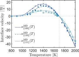
Figure 4. Crystallization velocity over temperature for silicon with the Stillinger–Weber potential, fitted by a Vogel–Fulcher equation (9).
Download figure:
Standard image High-resolution imageThe small velocity of the {111} interface is related to its dense packed structure and low energy, which does not provide favorable sites for the attachment of atoms. Therefore, a nucleation step has to take place before a new {111} layer can grow.
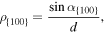
On the contrary, the {110} and {100} interfaces are rough because of the formation of {111} facets. Since the growth in these directions is not nucleation limited, it is faster, which is in agreement with results reported in previous studies [3, 43]. In figure 5 the atomic configuration of an {110} interface under growth conditions is shown. The formation of crystalline {111} can be clearly seen as well as the formation of faulted planes on these facets. As a rule of thumb, the relation between the maximum velocities  of the fitted curves is about 1:0.8:0.4 for this potential. The difference in growth velocity of {100} and {110} is related to the factor f in equation (4) since all other terms are bulk properties and not orientation dependent. To approach the factor f theoretically, we calculated the density of favorable sites by the density of {111} planes ending at a {100} surface. This is given by
where d is the distance of {111} planes and  the angle between the {111} and {100} plane. If one compares
  and
and  a relation of
  or 1:0.7 is found, which is in rough agreement with the relation derived from the simulation. Alternatively one can count the number of broken bonds per area at the surface, which gives an identical result.
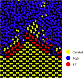
Figure 5. The atomic configuration of the {110} interface while crystal growth occurs. It is possible to see the rough character of the interface evidenced by the presence of {111} facets. Furthemore, stacking faults (SF) occur on these facets (red atoms). A similar behavior is observed for the {100} interface.
Download figure:
Standard image High-resolution imageCompared to literature values for MD simulations, we find values of 18–20 m s−1 for Stillinger {100} and 9–14 m s−1 for {111} [25, 28, 29], which is in good agreement with the above measured values. From experiments, velocities of 1.6 m s−1 are reported by Kuo [27] and 14 m s−1 by Ohdaira [34], so that we conclude that the results for the SW potential are a good representation of the anisotropic growth velocity of silicon crystals.
4. Atomistically informed phase field parameters
In this section, we derive the parameters for the phase-field model

where the one dimensional phase-field variable ![$p\,:{\mathbb{R}}\times (0,\tau )\to [0,1]$](https://content.cld.iop.org/journals/0965-0393/25/6/065015/revision2/msmsaa7862ieqn51.gif) varies between 0 and 1 to describe the two bulk states: liquid (p = 0) and solid (p = 1) and the interface region between the bulk states (
varies between 0 and 1 to describe the two bulk states: liquid (p = 0) and solid (p = 1) and the interface region between the bulk states ( ), as already mentioned in section 2.
Our main focus is that (10) reproduces the interface velocities calculated in section 3.4, while all parameters are carefully chosen, such that they are consistent with molecular dynamics with the SW potential. Since we have from molecular dynamics information about the three crystallographic orientations {100}, {110} and {111}, we also derive the model parameters for this orientations, which are indicated with the indices hkl in (10).
At the first step we derive the bulk free energy density F with the help of our molecular dynamical results described in section 3.2. In section 4.2, we incorporate interface energies from literature, which are also calculated via molecular dynamics with the SW potential. Finally, in section 4.3, we adapt the mobility parameter  , such that the model reproduces interface velocities from section 3.4, which we prove numerically in section 4.4.
4.1. Polynomial describing the bulk free energy density
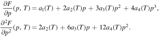
A free energy density  , which has the form of a double-well potential in p, can be established as a polynomial of fourth degree, which is one of the common forms for F. Here, the coefficients may depend on the temperature and we assume the expression

Since the equilibrium states for the bulk free energy density are represented by the two minima of the double-well polynomial, we choose the coefficients  , such that
  and
and  are the minima points of F. Then, we equip the free energy density F of the phase-field model with the equilibrium values of the atomistic free energy and via polynomial interpolation, such that we obtain two polynomials,
  for the crystalline values in figure 2 at p = 1 and
  for the amorphous/liquid values at p = 0. With respect to the condition, that f1 and f0 represent the minima of F, the free energy density has the form

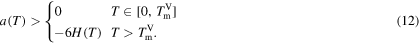
where  . Note here, that
  . For the remaining degree of freedom a(T) in (11) yields:
This expression for F fulfills  and
and  for the minima. Details of the derivation of (11) and (12) are given in the appendix A.1.
Furthermore, the maximum point of F is  with
with

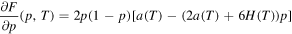
The calculation of (13) is described in appendix A.2. Hence, as we indicated in section 2, for the line g(p) which is tangent to both of the minima of F, the energy barrier Bkin, that has to be exceeded to get from one equilibrium phase to the other, is the difference of the function values of the maximum  and
and  . At the melting point TmV, the two minima of F have the same function value and thus
  is the difference of the function value of the maximum of F and the function value of the minima. Since the function values of the minima are then
  , with equation (13) the maximum point at TmV has the simple expression

Hence, the kinetic barrier at the melting point has the form

The kinetic barrier closely relates to the interface energy γ, which we discuss in section 4.2, where we also determine Bkin and hence with (14) the remaining degree of freedom for the bulk energy.
4.2. Interfacial free energy and width
We derive the gradient energy coefficient σ and the degree of freedom a in the free energy density (11) consistent with the interfacial energies obtained in Apte and Zeng [2], who used molecular dynamic simulations. We note that for the calculation of σ and a, we presently use only the values for the equilibrium state and hence make a independent on the temperature, since there is no literature with values of temperature dependent interface free energy calculated by means of molecular dynamics with SW potential for  . But after all, the mobility parameter
  will compensate the missing temperature dependence at this point.
Since Allen and Cahn [1], we know the relations between the interfacial energy coefficient σ in the PFM, the modeled interface thickness ε, the interfacial free energy γ and the modeled kinetic barrier Bkin.
At the melting point  the relations are
For convenience we set

For the crystal orientations {100}, {110} and {111}, Apte and Zeng [2] obtained the crystal-melt interfacial free energy γ, see table 3. We assume for orientation {111} an interface thickness of  and find a kinetic barrier of
  . Hence, the interface thickness of orientation {100} results in
  and of {110} in
  . In table 3, the values
  , and the resulting model parameters σ and a are given for all three considered orientations. Figure 6 shows the resulting double-well potential at different temperatures.
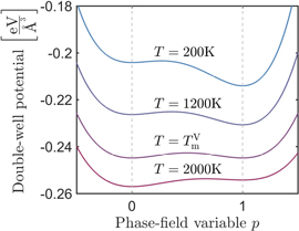
Figure 6. The double-well potential at different temperatures. At the melting point TmV, the two minima of the bulk free energy density have the same value.
Download figure:
Standard image High-resolution imageTable 3.
The crystal-melt interface free energies γ at the melting point TmV for the orientations {100}, {110} and {111} calculated by Apte and Zeng in [2]. With the help of γ and (15), we calculate the model constants a and σ for the three orientations. For that we choose an interface thickness of  for orientation {111}.
| Orientation | {100} | {110} | {111} |
|---|---|---|---|
 in eV Å−2 in eV Å−2 |
0.0262 | 0.0218 | 0.0212 |
 in Å in Å |
12.35 | 10.29 | 10 |
 in eV Å−1 in eV Å−1 |
0.8042 | 0.6702 | 0.6512 |
| a in eV Å−3 | 0.0339 | ||
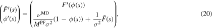
4.3. Realization of interface velocity in the phase-field model via the mobility parameter
In the previous subsections, we derived the bulk energy and the gradient energy of the phase-field model (10) by explicit use of the results from molecular dynamics. In this section, we calculate the mobility parameter  of the phase-field model (10), such that the model reproduces the atomistic velocities
  from section 3.4. But in the phase field, the interface velocity is not a parameter which can be directly incorporated as the interface energy
  in
in  or the free energy minima in F. Hence, we implement a shooting method, where we vary
  until all required conditions are fulfilled for a fixed temperature and orientation. This procedure is repeated for all three considered directions (100), (110) and (111), where we make measurements for the temperatures
  .
.
For the shooting method, we first define boundary values for (10), such that we have crystal material at the left boundary, and liquid material at the right:

We now fix the temperature and the orientation arbitrarily. Hence,  and also the velocity
  are constants. The phase field is a traveling wave solution and can be expressed as

Substitution of ϕ in (16) leads to the boundary value problem:

where  and
and  .
.
To receive an initial-value problem, we integrate the ordinary differential equation in (17) with the left boundary  , which holds as our first initial condition, and the right boundary s, which represents the new space-dependence variable for the shooting method. Furthermore, we define
  , thereby we are able to integrate the derivative of the potential F in ξ. For the calculation of the integral we use the second initial conditions
  . The both initial conditions guarantee, that we have crystal material at the left boundary. Applying all described conditions, we receive


By choosing  , our initial value problem has the form:


We calculate the mobility  via a bisection method. Therefore we vary
  until the right boundary condition
  is fulfilled for the numerical solution of (20)–(22). Thereby we solve the initial value problem with Runge-Kutta 4/5. We apply this method for each of the three orientations {100}, {110} and {111} and use the respective value of
  listed in table 3. Thereby we calculate
  for the respective temperature and orientation with the fits shown in figure 4. Our results are shown in figure 7 and listed in appendix A.3.
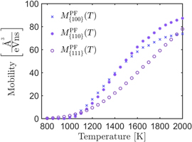
Figure 7. The extracted mobilities of the phase-field model as a function of temperature and orientation. The concrete values are listed in appendix A.3 in table A1.
Download figure:
Standard image High-resolution image4.4. Numerical solution of the phase-field model and velocity reproduction tests
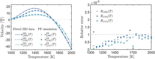
We solve model (10) numerically at fixed temperatures  for the three crystallographic orientations. During the simulation, we measure the velocity of the interface region by interpolating the position of p = 0.5. In fact, the model reproduces the velocities
  from molecular dynamics, see figure 8.
Figure 8. The points in the left figure are the mesured velocities from the numerical solution of equation (10) which we calculate with the Fourier-spectral method. The solid lines are the fitted velocities from molecular dynamics. Clearly, model (10) with the atomistic informed parameters reproduces exactly the kinetic inteface-behavoir. As shown in the right figure, only 5% of the relative errors of the velocities are greater than  . The highest error is about 0.0013 for the {110} orientatin at
  .
.
Download figure:
Standard image High-resolution image
As for the molecular dynamical simulations, we also have periodic boundary conditions for the phase-field model for  , which we solve numerically using a Fourier spectral method. Our equidistant grid guarantees that enough grid points are located on the interface to secure an accurate solution. For velocities close to zero, we lower the time step for a better result.
As initial condition we simply define a jump function J(x): for  we set J(x) equal to one close to the boundaries and zero in between. For
  we define J(x) the other way around. In both cases, one has to take care that the intervals where
  or
or  are wider than the interface thickness, else the system evolves to an equilibrium state before the traveling wave is established.
Our results of the numerical velocity measurement match accurately with the results from molecular dynamics. On the left-hand side of figure 8, the velocities from the phase-field simulation of model (10) are located directly on the line of the Vogel–Fulcher fit of the molecular dynamical data. For a better comparison, we calculate the relative error, which is
The relative error is shown on the right-hand side of figure 8. We observe, that the maximal relative error is 0.0013, which is at  for orientation {110}. 95% of the errors are even lower than 10−3.
5. Conclusion and outlook
In this study we have extracted the necessary parameters to obtain a phase-field model that can accurately describe the solid–liquid interface kinetics. In particular, using molecular dynamics simulations with the interatomic potential by SW, we derived an expression for the bulk free energy, the interfacial width of the liquid-crystal interface and the crystallization velocity and hence the corresponding anisotropic mobility parameter for three different orientations in silicon as a function of temperature. To properly capture the behavior of the temperature-dependent viscosity near the glass transition a Vogel–Fulcher fit is used for the SW potential. We show that these results are essential to obtain an accurate temperature dependence of the mobility parameter in the corresponding phase-field model for liquid-phase crystallization.
Our approach is presently being extended to two- and three-dimensional setting. Further extensions include the amorphous and poly-crystalline structure as well as defects such as stacking faults, in the free energy density and are expected to prove useful for validation against experimental results of  recrystallization in the future.
Acknowledgments
The authors gratefully acknowledge the fruitful discussions with Wei Cai and S Ruy and for pointing us to their software package. SB and DB acknowledge financial support by the Helmholtz Virtual Institute HVI-520 'Microstruc- ture Control for Thin-Film Solar Cells'. The authors are grateful for inspiring discussions with Dirk Peschka and Esteban Meca-Álvarez on modeling and numerical issues.
Appendix
A.1. Determination of the bulk free energy density F
Our approach for the free energy density is a polynomial of fourth degree in p

which attains the values in figure 2 at the equilibrium states p = 0 (liquid phase) and p = 1 (crystalline phase). So we need to consider the derivatives of F with respect to p:
From the conditions for the existence of minima at p = 0 and p = 1 follows


The polynomials  and
and  pass the equilibrium values in figure 2 for liquid/amorphous and crystalline
  , respectively. For the minima, we need for (A.1) the equalities
  and
and  and hence


With (A.4) and (A.7) the two coefficients a3 and a4 have the form


Together with (A.9) we can verify the inequality (A.5):

where the right-hand side of (A.10) is negative if and only if  , as one can observe in figure 2. Hence, for temperatures below the melting point, a2 has to fulfill (A.3). Finally, together with (A.8), (A.9), the double-well potential (A.1) has the form

where
The formulations (A.11) and (A.12) are equivalent to (11) and (12), respectively, by renaming  to a(T).
A.2. Derivation of the maximum argument μ
In the following, the calculation of μ is described, where the notation of (11) and (12) is used. We first note that with (12) we have

which can be seen easily by using the restrictions on a in (12):
First of all we note that for 

and for  ,
,

Besides that p = 0 and p = 1, the first derivative of F
has a third root 
Since (A.13) holds, the denominator of  can not become zero. Hence, with (12) we have
  . Further, the condition

is equivalent to

and together with (12) we have  for all
  . In addition, for a maximum in
  , the second derivative of F in
  has to be less than zero, i.e.

Since (A.13) holds, the denominator of (A.16) is negative and we get, since 

With (12), the last condition is a always true. Hence, the second derivative of F in  is less than zero, so
  is a maximum point of F.
A.3. Listed mobility values
In section 4.3 we describe the calculation of the mobility parameters for the phase-field model (10). The mobility values are shown in figure 7 and listed in table A1.
Table A1. The calculated mobilities via a shooting method for orientations {100} {110} and {111}. They are shown in figure 7.
| Temperature | Mobility 
|
Mobility 
|
Mobility 
|
|---|---|---|---|
| T in K | in Å3 (eV ns)−1 | in Å3 (eV ns)−1 | in Å3 (eV ns)−1 |

|
0 | 0 | 0 |
| 800 | 8.8818 × 10⁻¹⁴ | 8.8818 × 10⁻¹⁴ | 2.93 × 10⁻¹ |
| 850 | 9.7105 × 10⁻⁸ | 1.7795 × 10⁻⁹ | 5.6933 × 10⁻¹ |
| 900 | 5.8741 × 10⁻³ | 8.4051 × 10⁻⁴ | 1.0082 |
| 950 | 2.2923 × 10⁻¹ | 6.8938 × 10⁻² | 1.658 |
| 1000 | 1.425 | 6.2816 × 10⁻¹ | 2.5636 |
| 1050 | 3.3476 | 1.8627 | 3.761 |
| 1100 | 6.8805 | 4.4784 | 5.2861 |
| 1150 | 11.4558 | 8.3461 | 7.1611 |
| 1200 | 16.737 | 13.2755 | 9.4112 |
| 1250 | 22.4071 | 18.9898 | 12.0447 |
| 1300 | 28.2093 | 25.213 | 15.06 |
| 1350 | 33.9597 | 31.7057 | 18.4506 |
| 1400 | 39.5291 | 38.274 | 22.2025 |
| 1450 | 44.8397 | 44.7766 | 26.3002 |
| 1500 | 49.7514 | 51.0148 | 30.6662 |
| 1550 | 54.1681 | 56.8348 | 35.2213 |
| 1600 | 58.1903 | 62.2964 | 39.9958 |
| 1650 | 61.8892 | 67.4445 | 45.0044 |
| 1700 | 63.6398 | 70.4575 | 48.9622 |
| 1750 | 66.429 | 74.5941 | 54.0443 |
| 1800 | 68.8907 | 78.3509 | 59.2121 |
| 1850 | 70.7543 | 81.4046 | 64.1717 |
| 1900 | 71.9325 | 83.6335 | 68.749 |
| 1950 | 72.9413 | 85.6235 | 73.3545 |
| 2000 | 73.6987 | 87.2768 | 77.8687 |