

Abstract
Surfaces and interfaces are of particular importance for optoelectronic and photonic materials as they are involved in many physical and chemical processes such as carrier dynamics, charge transfer, chemical bonding, transformation reactions and so on. Terahertz (THz) emission spectroscopy provides a sensitive and nondestructive method for surface or interface analysis of advanced materials ranging from graphene to transition metal dichalcogenides, topological insulators, hybrid perovskites, and mixed-dimensional heterostructures based on 2D materials. In this review paper, we start with the THz radiation mechanisms under ultrafast laser excitation. Then we concentrate on the recent progresses of THz emission spectroscopy on the surface and interface properties of advanced materials, including transient surface photocurrents, surface nonlinear polarization, surface states, interface potential, and gas molecule adsorption/desorption processes. This novel spectroscopic method can not only promote the development of new and compact THz sources, but also provide a nondestructive optical method for surface and interface characterization of photocurrent and nonlinear polarization dynamics of materials.
Export citation and abstract BibTeX RIS
1. Introduction
Chemical bond formation, charge transfer, matter transfer, and many reaction processes of materials are governed by the chemistry at the surface, hence Nobel laureate Pauli once said 'God made the bulk; surface were invented by the devil' [1]. Moreover, the dynamic processes of electrons, holes, dipoles, and some quasi-particles in optoelectronic devices are controlled by the physics at the interface, hence Nobel laureate Herbert Kroemer said 'the interface is the device' [2]. Optical methods have been widely used for characterizing the surface and interface properties of materials due to their nondestructive, fast, sensitive, and spatially resolved detection. For instance, in 1980s, surface plasmon resonance spectroscopy based on linear reflectivity measurement has been developed into an efficient label-free and real-time quantification measurement of dielectric property [3] and chemical or biomolecular interaction kinetics [4, 5]. Similarly, in the later 1980s, nonlinear optical spectroscopy such as second harmonic generation and sum-frequency generation spectroscopies have been developed successfully by Shen et al for the surface and interface property studies such as solid surface/interface adsorption, liquid surface/interface monitoring, and in situ remote sensing [6, 7]. Such optical techniques are capable of detecting a monolayer of molecules at surface and applicable to all interfaces in optical penetration accessible by light. As such, the development of optical characterization tool for surface and interface is an important and interdisciplinary research, which connects the linear/nonlinear optics with surface physics and opens a new chapter of surface and interface research for material science and condensed matter physics. However, most of optical methods for surface/interface information solely focus on intensity interrogation, it is desirable to develop a spectroscopy tool with rich spectroscopic information to gain a deep insight into the surface/interface properties of materials.
Terahertz (THz) surface/interface emission spectroscopy is another optical method, which was considered as a potential tool for the optoelectronic measurement of traditional semiconductor at surfaces and interfaces proposed by Zhang et al [8]. Under ultrafast laser excitation, transient carriers, dipoles, phonons, excitons, and other quasi-particles are firstly generated at the surfaces and interfaces of materials. Such photoexcited species change instantly and further induce THz radiation pulses in a picosecond (ps) scale. The recorded THz radiation carry rich information [9, 10] in the THz waveforms such as amplitude, phase, polarity, and polarization, which are sensitive to doping type, carrier mobility, carrier concentration, excess energy, nonlinear susceptibility, and so on. This physical process is also sensitive to the surface and interface properties such as surface crystalline symmetry, surface carrier distribution, surface band bending, surface/interface potential, surface depletion field etc. These properties are superior to optoelectronic devices and condensed matter material characterization at surfaces and interfaces. Therefore, optoelectronic properties of a broad range of traditional materials are probed via THz emission spectroscopy. For example, ultrafast photoexcited carrier dynamics in InP [11], polarization of virtual photocarriers in GaAs [12], hot carrier mobility and transient surface conductivity of InSb [13], ultrafast buildup of photo-Dember field of InAs [14], and the dynamics of nonlinear processes at gold and silver surfaces [15] have been reported.
In contrast with the traditional materials, new emergent advanced materials such as graphene, metal transitional dichalcogenides (TMDs), topological insulators, and organic–inorganic hybrid perovskites have been developed since the 21st century. These materials demonstrate rich information at surfaces and interfaces as most of them are layered materials with the dominant optical physics by surface or interface states rather than by bulk states. Compared with traditional materials such as GaAs, InP etc, these advanced materials usually are formed by in-plane covalent bonding and out-of-plane van der Waals (vdW) interaction, which are readily to be made into two-dimensional (2D) single layer material by physical exfoliation [16], liquid phase exfoliation [17–19] or chemical vapor deposition [20] from small size to large scale. These materials show ultrahigh surface atoms without dangling bonding [21], which provide ideal platforms to study the physical and chemical properties of carriers, dipoles, and quasi-particles at surfaces and interfaces. The electric band structures of these advanced materials range from metal, semimetal, through semiconductor (in visible and infrared region) to superconductor [22], which have opened a whole new era of 2D electronics and photonics connected with novel concepts and potential applications [23–25]. These applications further promote the development of vallytronics [26, 27], spintronics [28], excitonics [29, 30] and plasmonics [31–34]. Furthermore, it is easy to fabricate vdW heterostructures of these advanced materials without lattice matching and with atomic sharp potential field gradient [35]. These heterostructures boost wealthy phenomena such as energy transfer, charge tunneling, electron reconstruction, proximity effect etc, which can be further used for band-structure engineering of the materials [36]. Finally, surface and interface engineering of these advanced materials such as surface/interface atom modification, element doping, intercalation, strain, and electric/magnetic fields [37] have opened up a new paradigm for the designation of high-performance optoelectronic devices [35].
With the development of advanced materials and THz technology, THz emission spectroscopy is developing towards two directions. On the one hand, the discovery of new THz sources based on new physical processes in these emergent advanced materials is desirable for integrating 2D THz photonics as the THz region (0.1 THz to 10 THz) is still the least studied electromagnetic wave spectral region, which is viewed as 'THz gap' [38]. On the other hand, THz emission spectroscopy has become a sensitive and nondestructive inspection tool for condensed matter physics studies such as the evolution of surface state in Bi2Se2Te [39], dynamics of Dirac fermions of surface state in Bi2Se3 [40], transient photocurrents in graphite [41], built-in electric field along aligned carbon nanotubes [42], and dynamic photon drag effect (PDE) in monolayer [43] and multilayer graphene [44]. Such surface and interface property investigations unveil the optical physics of various advanced materials and supplement the surface and interface characterization by other optical methods.
Herein, we present a snapshot of recent progresses of the surface/interface THz radiation from advanced materials by the femtosecond (fs) laser excitation. Firstly, the THz emission spectroscopy system and several THz radiation mechanisms are briefly introduced. Then we summarize the recent progresses of surface photocurrent in graphene, surface nonlinear polarization and photocurrent surge in TMDs, surface states and photocurrents in topological insulators, transient photocurrents in hybrid perovskites, and interface potential as well as gas adsorption/desorption processes in mixed-dimensional heterostructures with THz emission spectroscopy. Finally, we describe the challenge and perspective of the THz emission spectroscopy for material characterization at surfaces and interfaces in the future.
2. THz emission spectroscopy system
THz emission spectroscopy is an analogy to the traditional THz time-domain spectroscopy, but the measured samples are used as THz emitters instead of using ZnTe (1 1 0) or GaAs (1 0 0) as the THz emitters to study the THz response such as dielectric constant [45] and excitonic dynamics [46] of materials in THz region. The transient THz signal after the fs laser excitation is related to the carrier mobility, built-in potential, crystalline symmetry, nonlinear susceptibility, transient photocurrent, adsorption/desorption energy etc, which can be reflected in the change of the amplitude, phase, polarity, polarization of THz radiation, as well as the dependence on pump power, azimuthal angle, and incident polarization angle.
2.1. THz emission spectroscopy system
Figure 1(a) demonstrates a schematic of THz emission spectroscopy system. An ultrafast laser with fs pulse duration is usually used as a laser source. The pulses are divided into two parts via a beam splitter. The transmitted beam with the majority of the pulse energy is used to pump samples, from which the emitted THz pulses are collected, collimated, and focused onto a detection crystal such as ZnTe (1 1 0) by a pair of parabolic mirrors. At the same time, the probe beam with the minority of the pulse energy is focused onto the detection crystal and overlaps with the pump beam. Then the generated THz radiation can be detected and recorded by an electro-optical sampling technique [47], and the parallel and perpendicular components of the THz radiation can be extracted with the help by a pair of wire-grid polarizers [48].

Figure 1. (a) Schematic of a THz emission spectroscopy system, where the reflection configuration can be switched to the transmission configuration via a flip mirror M1. The HWP (half-wave plate) and GTP (Glan–Taylor prism) are used to change the polarization state of the probe beam. A combination of polyethylene and silicon plates are placed behind the sample to scatter and block the residual pump pulses, while the generated THz pulses can pass through them with negligible absorption. (b) Typical THz time-domain signal. (c) Amplitude and (d) phase of the THz signal in frequency domain after Fourier transformation of the time-domain signal.
Download figure:
Standard image High-resolution imageFigure 1(b) depicts a THz radiation signal oscillating in ps time scale, of which both amplitude and phase spectra in frequency domain are derived after Fourier transformation of the time-domain signal (figures 1(c) and (d)). The full width at half maximum in amplitude spectrum represents bandwidth of the THz emitter, which is related to the dynamics of the photoexcited species in the samples and the detection bandwidth of the THz system. The detection bandwidth of the THz system can be improved via different electro-optical crystals with wide bandwidth such as GaP and GaSe [49]. Laser-induced plasma [50] and photoconductive antenna [51] are also alternative detection methods with broad detection bandwidth.
2.2. THz radiation mechanism under ultrafast laser excitation
In general, THz radiation is related to the time derivative of the photogenerated carriers or the polarization/magnetization by the ultrafast intensive laser pulses, which can be described as follows:

where  is the nonlinear polarization,
  is the photocurrent density, and
  is the magnetization. Here, we mainly discuss the nonmagnetic materials with
  or
or  , while the THz radiation from magnetic materials are discussed in the previous review [52]. The nonlinear polarization refers to the optical rectification process (figure 2(a)) when the incident photon energy is below the bandgap of materials [53]. The incident photons can induce a low frequency electric field via difference-frequency generation. Such process is described by the nonlinear dielectric polarization P (Ω) as:
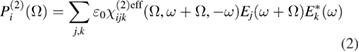
where  is an effective second-order nonlinear susceptibility and ω is fundamental angular frequency. Due to the symmetry, this second-order nonlinear optical effect can only exist in non-centrosymmetric materials. However, as the surface or interface will break the bulk symmetry materials, this optical rectification process can also happen at the surface or interface. The strength of optical rectification is directly relevant to the nonlinear optical coefficients of materials. Early studies focusing on the THz radiation from LiNbO3 [54], ZnTe [55], GaSe [56], and organic crystal dimethyl amino 4-N-methylstilbazolium tosylate [57] make great contributions to the development of THz time-domain spectroscopy. Moreover, a surface depletion field will enhance the optical rectification, which can also happen in centrosymmetric materials. Different from the bulk optical rectification, the effective nonlinear susceptibility of surface optical rectification with the help of the surface electric field is expressed as:
  [58, 59], where
  is a third-order susceptibility tensor and
  is the surface depletion field. The bulk and surface optical rectification contributions can be distinguished according to the THz radiation as a function of azimuthal angle, i.e. rotational symmetry of a crystalline surface as the difference between nonlinear susceptibility tensors will lead to different nonlinear polarization and azimuthal angle dependence.
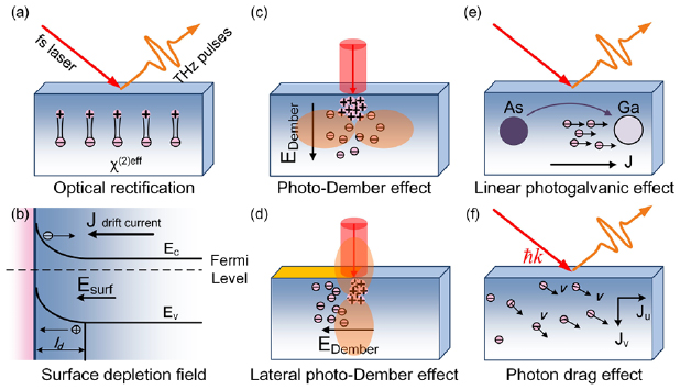
Figure 2. Schematic illustrations of physical processes at surfaces and interfaces to generate THz radiation. (a) Optical rectification effect. (b) Surface depletion fields represented by n-type semiconductors with upward band bending, while downward band bending occurs in p-type semiconductors. (c) Photo-Dember effect and (d) lateral photo-Dember effect, which is introduced via adding a metallic strip on the material surface. The orange dumbbells indicate the THz radiation pattern from effective dipoles in photo-Dember fields. (e) Linear photogalvanic effect (PGE) represented by GaAs crystal. (e) PDE due to the momenta transfer from photons to electrons.
Download figure:
Standard image High-resolution imageWhen the incident photon energy is above the bandgap of materials, photogenerated carriers will accelerate under intrinsic electric fields and further induce THz radiation. Surface depletion field is one of the intrinsic fields induced by the band bending at the surface as shown in figure 2(b). Both conduction and valence bands bend due to the Fermi level difference between surface and inferior region of semiconductor. This surface field will introduce the photocurrent surge, which is among the earliest THz radiation mechanism of semiconductor materials [11]. Such process often occurs in semiconductors with wide band-gap, such as GaAs (1.43 eV), InP (1.34 eV), and CdTe (1.4 eV). Figure 2(b) demonstrates n-type semiconductors with the upward surface band bending, while p-type semiconductors will bend downwards. This difference of band bending in n-type and p-type semiconductors will reverse the polarity of THz time-domain signal as the photocarriers in n-type and p-type semiconductors accelerate along opposite directions [11, 60]. Moreover, the surface electronic states of materials can be modified by surface engineering with physical or chemical methods such as introducing surface roughness [61], coating metallic film [62], and chemical passivation [63]. This modification will change the surface depletion field and the quantum yield of photocarriers in materials, which will be reflected in THz radiation signal. From the variation of the THz radiation signal combined with THz radiation models, the nature of surface field, band bending, and carrier transport dynamics can be obtained by THz emission spectroscopy.
In narrow band-gap semiconductors such as InAs (0.36 eV) and InSb (0.17 eV), significant difference between electron and hole mobility will introduce the separation of the photoexcited electrons and holes at the surface as shown in figure 2(c). This separation will introduce the diffusion photocurrent due to the concentration gradient of photocarriers from the surface to the bulk, and the drift photocurrent under the Dember electric field [64]. This process is the so-called photo-Dember effect, of which the Dember electric field is perpendicular to the surface and the THz radiation pattern is parallel along the surface as indicated with the orange dumbbells in figure 2(c). This suggests that to detect THz signal, it will be better to set the experiments at oblique incidence and in the reflection geometry (as shown in figure 1(a)) so that the carrier gradient and the resulting THz radiation pattern are tuned with an angle to the surface. If the surfaces are modified by metallic particles or strips as shown in figure 2(d), a strong photocarrier gradient parallel to the surface can be formed [65, 66]. This will introduce a lateral photo-Dember field with the photocurrent along the surface and the THz radiation perpendicular to the surface. With the lateral photo-Dember effect, THz radiation can be observed from GaAs (1 0 0) surface coated with rough gold film at normal incidence [62]. This lateral photo-Dember effect can be used to enhance THz radiation from traditional GaAs photoconductive switches [66].
Based on second-order nonlinear processes, photogalvanic effect (PGE) and PDE can generate transient photocurrent from real carriers under resonant excitation (above bandgap) instead of nonlinear polarization of virtual carriers under nonresonant excitation (below bandgap) [53, 67]. These two effects can also introduce THz radiation. Take linearly polarized excitation as an example, linear PGE originates from the spatial charge transfer during the transition from valence band to conduction band in non-centrosymmetric materials (figure 2(e)), hence the resulting photocurrent flowing along the inherent polar direction in materials. PGE can occur in any materials with a polar axis or without inversion symmetry, and the photocurrent is controlled by the crystalline symmetry of materials [68]. This is different from the photocurrent surge governed by either surface electric field or spatial carrier inhomogeneity.
However, the PDE arises from the momentum transfer from the incident photons to the electrons near the surface in the penetration depth as shown in figure 2(f). The charge carriers in materials will move along the direction of the incident light and generate transient photocurrent, and thus the PDE is related to the incident wave-vector. In contrary to the PGE, the PDE is not restricted by inversion symmetry of materials, and it usually happens in materials with rich free carriers such as doped semiconductors and metal. The photocurrent density from PGE and PDE effects can be expressed as [69, 70]:
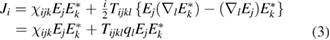
where E is the complex electric field of pump beam; q is the incident wave vector;  and
and  are third and fourth order susceptibility terms describing the PGE and PDE, respectively. According to equation (3), the photocurrent introduced by the PDE is directly related to the wave vector q while that from the PGE is independent on q, hence the contributions from such two effects on photocurrent generation and THz radiation can be distinguished via changing the propagation direction of pump beam [70].
3. Surface/interface properties probed by THz emission spectroscopy
In recent years, the advanced materials are discovered to exhibit unprecedented physical and chemical properties at surfaces and interfaces such as planar conductivity, surface activity, magnetic anisotropy, charge tunneling, charge hopping, and so on [37]. THz emission spectroscopy as a sensitive probing method has realized in-depth studies of the fundamental properties of advanced materials such as nonlinear optical response, photocarrier dynamics, surface state, and surface/interface engineering, which can not only fertilize the surface/interface physics of the advanced materials, but also provide important assets for future applications in photonics and optoelectronics.
3.1. Surface photocurrents in graphene
As one of typical 2D materials, graphene has a linear dispersion relation [71], a high electron mobility (~2.5 × 105 cm2 V−1 s−1 at room temperature) [72], fine structure constant determined optical absorption (πα ≈ 2.3%) [73], and many other remarkable properties. In THz region, negative photoconductivity with the transient response on a time scale of 1–2 ps in highly doped monolayer graphene was observed via optical pump THz probe spectroscopy (OPTP) [74–76]. This phenomenon is ascribed to the increase of scattering rate (Г), of which the contribution is more significant than that from the Drude weight (D) in the real part of the conductivity ( ) [74]. Further experiments with the gate-tuned carrier densities suggest positive photoconductivity near the charge neutrality point and negative photoconductivity at high carrier density, which is due to the interplay between photoinduced changes of both D and Г [76]. Under different optically doping density and different excitation photon energy, hot carrier and multiple hot-carrier generation have been observed with the dynamics dominated by carrier-carrier scattering instead of carrier-optical-phonon scattering [75, 77]. These scattering processes are crucial for the conversion of light into free electron–hole pairs and the consequent photocurrent formation in graphene [75]. As the carrier dynamics of graphene exhibit sensitive, broadband, tunable, and ultrafast response [78], graphene has many applications in THz region, such as THz detector [79], THz modulation [80], THz antireflection coating [81], THz modulators [82, 83], and so on. As proposed by Novoselov et al in the graphene roadmap for future photonic applications [84], graphene based THz generators are also very promising in the 2D photonics for the integration. Early studies suggested ballistic electric currents in graphene could induce the coherent THz radiation using quantum interference of one- and two-photon absorption pathways [85]. In 2012, Prechtel et al [86] demonstrated photocurrent induced THz radiation in a graphene–metal interface by photocurrent measurement, and revealed two dominant mechanisms of the photocurrent generation. One is carrier separation by a built-in electric field due to potential difference between layers, and the other is photothermoelectric effect (PTE) due to thermoelectric power difference [87]. PTE originates from a temperature gradient generated by light across an interface, where hot carriers tend to diffuse to maximize the entropy and thus the carrier flowing results in the transient photocurrent. In recent years, the THz radiation investigations of monolayer graphene [43], multilayer graphene [44, 48, 69], and vertical grown graphene [70] indicate that PDE dominates the transient photocurrent generation of graphene deposited on dielectric substrates. As shown in figure 3(a), when a graphene sample is excited by fs laser, momenta of the incident photons are transferred to those of electrons in the graphene, which drives the electron flowing along the propagation direction of the photons. This current flow further induces transient photocurrent, resulting in THz radiation at graphene surface [43]. Based on equation (3), the photon drag currents are determined by the electric components of the incident lasers, and thus the photocurrent components have dependences on the incident polarization angle α as:
  , and
, and  . Since x- and y -components of the generated THz radiation (with the coordinate system shown in figure 3(a)) depend on the photocurrent components as:
  ,
,  , the THz radiation components have dependences on the incident polarization angle as:
  , and
, and  . These relations are consistent with the experimental results as shown in figures 3(b) and (c), verifying the dominant contribution of PDE for transient photocurrent generation in graphene. In this way, THz emission spectroscopy provides a contactless tool for probing the ultrafast photocurrent without electrodes, which would be superior to the conventional photocurrent measurement as it is based on a digital oscilloscope with external electrodes and limited time resolution and bandwidth [48].

Figure 3. (a) Transient photocurrent distribution and induced THz radiation of monolayer graphene under femtosecond (fs) laser excitation. (b) and (c) are x- and y -components of the generated THz signals as a function of incident polarization angle α shown in (a). (d) Transient nonthermal electron and hole population distributions of graphene, which are symmetric with respect to the center of the Dirac cone under normal excitation while asymmetric under oblique excitation. (e) and (f) are THz emission spectroscopy of graphene in time and frequency domains, where the upper (green lines) and bottom (red lines) layers represent experimental and calculated results, respectively. (a)–(c) Reprinted with permission from [43]. Copyright 2014 American Chemical Society. (d)–(f) Reprinted with permission from [44]. Copyright 2014 American Chemical Society.
Download figure:
Standard image High-resolution imageTo gain a deep understanding of transient photocurrents in graphene, Maysonnave et al demonstrated the microscopic physics of dynamic PDE according to the carrier distributions after fs laser excitation [44]. As shown in figure 3(d), the populations of nonthermal electrons and holes are asymmetric along the center of Dirac cone when graphene is under oblique incident illumination. This will drive carrier motions and induce transient net current, which results in the THz radiation. While the populations of electrons and holes are symmetric along opposite wave vectors at normal incidence, hence the momentum contributions cancel with each other and could not emit THz radiation. This microscopic mechanism is based on a tight-binding model, and the density matrix ρ evolution in the standard perturbation formalism as [44]: ![${\rm i}\hbar \partial {{\rho }^{(n)}}/\partial t=\left[ {{H}_{0}},{{\rho }^{(n)}} \right]+\left[ {{V}_{{\rm dip}}},{{\rho }^{(n-1)}} \right]-{\rm i}\hbar {{\Gamma }_{n}}{{\rho }^{(n)}}$](https://content.cld.iop.org/journals/0953-8984/31/15/153001/revision2/cmab00c0ieqn019.gif) where n = 1, 2 is the order number;
where n = 1, 2 is the order number;  is the phenomenological damping;
  is the dipolar perturbation. The photocurrent induced THz radiation is proportional to the time-derivative of the second-order current [44]:
 ![${{\vec {E}}_{{\rm THz}}}(t)\propto \partial Tr\left[ \vec {p}{{\rho }^{(2)}} \right]/\partial t$](https://content.cld.iop.org/journals/0953-8984/31/15/153001/revision2/cmab00c0ieqn022.gif) where Tr is the trace operation;
where Tr is the trace operation;  is the momentum. Thus, the calculation of the THz radiation is governed by the diagonal elements of
  , which reflects the transient electron and hole nonlinear populations induced by the pump laser. Based on this theoretical model, the THz signals are reproduced and consistent with the measured THz signals in both time and frequency domains, as shown in figures 3(e) and (f). Furthermore, the calculated THz spectrum indicates that nearly 60 THz bandwidth signal is generated when graphene is excited by 15 fs pulse laser, making graphene a candidate as a compact and ultrabroadband THz emitter. Regarding the microscopic mechanism of the PDE, THz emission spectroscopy is also a new way to probe the dynamics of nonequilibrium carrier populations.
3.2. Surface nonlinear polarization and photocurrent surge of transitional metal dichalcogenides
As another kind of advanced materials, TMDs present complementary yet distinctive properties compared with graphene. TMDs possess sizable bandgaps which can change from indirect to direct when TMDs are tuned from few-layer or bulk structures to monolayer structures [88, 89]. The strong spin–orbit coupling from d orbitals of heavy metal atoms endows TMDs new physics in spintronics and valleytronics [28]. Besides, TMDs have strong excitonic effects due to large exciton binding energy and low dielectric screening of Coulomb interactions between charge carriers [90, 91]. In THz region, TMDs also present extraordinary optoelectronic properties. For instance, both free carriers and bounded excitons are observed in tungsten diselenide (WSe2) by OPTP [92], and the transient THz photoconductivities of monolayer molybdenum disulfide (MoS2) and WSe2 reach ultrafast response time of 350 fs and 1 ps, respectively [93]. Negative THz photoconductivity was observed in doped monolayer MoS2 due to strong many-body interaction, which converts the 2D electron gas into a charged trion gas [94]. However, the widely used OPTP or THz time-domain spectroscopy is limited to achieve the surface and interface research on TMDs. Yet, surface/interface characterization is essential to device performances in photonic and optoelectronic applications.
Using THz emission spectroscopy, we observed resonant optical rectification process in the surface region of layered MoS2 crystal [95]. The optical rectification process is confined to an interactive volume above the crystalline surface (at Z = 0 in figure 4(a)). In this process, the generated THz radiation is proportional to the second order time derivative of the nonlinear polarization as:  , which gives rise to an azimuthal angle (φ in figure 4(a)) dependence of THz radiation as the nonlinear susceptibility tensor and the nonlinear polarization are related to φ. As such, the optical rectification induced THz radiation as a function of φ can be expressed as [95]:

where d22, d15, d31, and d33 are effective nonlinear coefficients, and the 3φ rotational symmetry agrees well with the experimental results as shown in figure 4(b). This indicates that although the hexagonal 2H–MoS2 is centrosymmetric belonging to D6h space group, the surface breaks the bulk symmetry and thus the nonlinear effect on the surface obeys the three-fold rotational symmetry. Different from the azimuthal angle dependence, the THz amplitude as a function of the incident polarization angle (α in figure 4(a)) exhibits 2α rotational symmetry (as shown in figure 4(c)) as [96]:  , where A, B, C, D, and E are fitting constants related with the nonlinear coefficients. This is due to that the nonlinear polarization is given based on the interaction between susceptibility tensor and the incident electric field according to equation (2). The azimuthal angle contributes to the variation of susceptibility tensor, while the polarization angle changes the incident electric field. Hence the nonlinear polarization and the induced THz radiation have different dependences on the azimuthal angle and incident polarization angle.

Figure 4. THz surface emission from layered MoS2 crystal. (a) Diagram of crystalline surface under fs laser excitation (incoming arrow) and generated THz pulses (outgoing arrow) in the reflection configuration. θ and α are incident angle and polarization angle of the pump beam, respectively. The bottom layer is the microscopic illustration of the azimuthal angle φ on the surface of the layered MoS2 crystal. THz amplitude as a function of the (b) azimuthal angle φ and (c) polarization angle α. (d) and (e) THz radiation from MoS2 crystal in the transmission configuration, where (d) and (e) are THz amplitude as a function of the incident polarization angle at normal and oblique incidences, respectively. The purple arrow indicates the amplitude shift from zero baseline. (a)–(c) Reprinted with permission from [95]. Copyright 2017 American Chemical Society. (d) and (e) Reprinted with permission from [96]. Copyright 2018 American Chemical Society.
Download figure:
Standard image High-resolution imageIn general, several competing physical processes happen simultaneously when the advanced materials are excited by the pump beam. Thus, we have also investigated new emergent physical processes of MoS2 by THz emission spectroscopy with the transmission configuration as the reflection configuration has a limitation on steering an incident angle [96]. As shown in figures 4(d) and (e), the THz radiation at −40° incidence increases and significantly shifts toward the positive direction (indicated by the purple arrow in figure 4(e)) compared with the values at normal incidence. Such shift mainly stems from the THz radiation contribution induced by photocurrent surge. Since the photo-Dember effect is negligible in MoS2 due to the same order of magnitude for mobility and masses between electrons and holes, origin of the photocurrent surge is ascribed to the surface depletion field. This surface depletion field with ~0.13 µm in the penetration depth forms near the air–MoS2 interface, and the maximum value of the surface depletion field is approximately 1.45 × 10⁴ V cm−1. Comparing the physical processes at MoS2 surfaces, the resonant optical rectification is related to the nonlinear susceptibility and can be influenced by the crystalline symmetry i.e. the azimuthal angle, while the surface depletion field is associated with surface potential and carrier concentrations, and it is independent on the azimuthal angle. Thus, the THz radiation contribution from resonant optical rectification and from surface depletion field were estimated according to the azimuthal angle dependence of the generated THz signals. The results indicate that the contribution from resonant optical rectification decreases from 90% to 40% with the incident angle changing from 0° to −40° [96].
Tungsten disulfide (WS2) is an analog to MoS2 due to their similar electronic structure and physical properties. However, we observed that the dominant physical process of WS2 in THz emission is different from that of MoS2 [97]. As shown in figure 5(a), the generated THz signals of layered WS2 crystal are insensitive to the azimuthal angle and demonstrate an isotropic response in the polar coordinate, suggesting different features from the 3φ rotational symmetry of MoS2. With respect to the incident polarization angle, the THz signals of WS2 and MoS2 both exhibit 2α rotational symmetry as shown in figure 5(b). Nonetheless, the amplitude modulation of MoS2 is much larger than that of WS2 and the THz amplitude of WS2 shifts significantly towards positive direction. These azimuthal- and polarization-angle-insensitive properties of THz radiation from WS2 suggest that the photocurrent surge rather than the nonlinear polarization governs the physical mechanism of THz radiation in WS2. This is primarily due to the difference of nonlinear coefficients between MoS2 and WS2. According to equation (4), sin(3φ) term is related to the coefficient d22, while the azimuthal-angle-independent terms contain coefficients d15, d31, and d33. The calculated nonlinear optical coefficients indicate that d22 is the largest coefficient among nonzero susceptibility terms of MoS2 and other terms are almost zero [96], while d22 of WS2 is approximately zero (figure 5(c)) and further results in the isotropic behavior for THz radiation. Thus, the dominant mechanism of THz radiation from WS2 is photocurrent surge (contribution ratio ~88%), which is induced by the surface depletion field rather than photo-Dember effect since the mobility and masses of electrons and holes are almost identical in WS2. The maximum value of the depletion field is calculated as 1.2 × 10⁵ V cm−1 with approximately 94 nm width. Moreover, the THz emission spectroscopy of layered WSe2 crystal presents similar features with WS2 including azimuthal angle independent THz radiation, weak modulation of incident polarization angle, and the THz amplitude shift towards positive direction. Thus the surface depletion field also plays an important role for the photocarrier acceleration and THz radiation in WSe2 [98].

Figure 5. Comparison of the THz radiation from WS2 (squares) and MoS2 (pentagons) as a function of (a) azimuthal angle and (b) polarization angle. The red arrow indicates the upward shift of the THz amplitude of WS2 compared with that of MoS2. (c) Calculated nonlinear optical coefficients of WS2 by first-principle method. The red dashed line denotes the position of 800 nm (1.55 eV) pump beam. Reprinted figure with permission from [97], Copyright 2019 by the American Physical Society.
Download figure:
Standard image High-resolution image3.3. Surface states and photocurrents in topological insulators
Topological insulators have become the 'star material' after graphene in optics, electronics, condensed matter physics, and so on [99] due to their unique properties such as narrow bandgap in bulk and nearly linear energy-momentum dispersion relationship at the surface, time-reversal symmetry protected surface, and strong spin–orbit interaction at surface states [40, 100]. What's more, with the existence of Dirac cone-like surface state, surface photocurrents with ps timescale can be induced in topological insulators after optically excited by fs laser. Thus THz emission spectroscopy enables in-depth studies of the surface state, Dirac fermions, and photocurrent distributions of topological insulators. Luo et al pointed that the THz radiation generated inside a bulk Bi2Se3 experienced a free carrier absorption, of which Dirac fermion contribution is more efficient than the carrier contribution from the bulk [40]. Zhu et al [101] and Tu et al [102] demonstrated that the energy difference between a second Dirac surface state and bulk bands matches the 1.55 eV photon energy of excitation wave, which are essential for photoexcited carriers at surface resulting in THz radiation. Choi et al observed that the THz polarities of an as-grown Bi2Se2Te and annealed samples are opposite. This is due to that Bi2Se2Te sample can be transformed from amorphous film with p-type polarity into single crystalline Bi2Se2Te1 with n-type polarity via annealing process, revealing the surface depletion field contribution to the THz radiation [39].
Furthermore, Braun et al quantitatively extracted the ultrafast photocurrent components Jx and Jyz in Ca-doped Bi2Se3 by THz emission spectroscopy [103]. Firstly, a THz electric field E(t) is extracted from the measured THz signal S(t) by deconvolution of the system response function h(t), which has the relationship in the frequency domain as:  . This relation is also applied in Eyz component. Secondly, THz electric fields due to the photocurrents are given through generalized Ohm's law in the frequency domain as [104]:
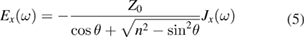
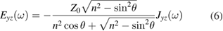
where Z0 ≈ 377 Ω is vacuum impedance; n is refractive index of Bi2Se3; θ = 45° is incident angle. Finally, the time-resolved photocurrent components are portrayed after inverse Fourier transformation of the current spectra as shown in figure 6(a). The physical origin of the photocurrent components can be understood based on the established THz radiation mechanisms: shift current, injection current, and optical rectification, which are proposed by Sipe et al [105] and Driel et al [53] for the photocurrent generation by an optical transition |i 〉 → |f 〉. Among them, optical rectification has been demonstrated in figure 2(a), and injection currents arise from the asymmetric band depopulation since the electrons are excited from the Dirac cone to higher-lying states with different group velocity under circularly polarized excitation (figure 6(b)). While shift currents are caused by the spatial shift of electron density distribution along Se-Bi bond when electrons are excited from state |i 〉 to |f 〉 (figure 6(c)). Although both the injection and shift currents follow the waveform of optical pulse, the characteristic shape of the injection current is unipolar while the shape of the shift current is bipolar. Regarding to the portrayed photocurrent components, Jx with relaxation time τ ~ 22 fs has bipolar waveform, which is consistent to the theoretical photocurrent waveform based on the shift current model (dash line in figure 6(a)). Thus, Jx component is caused by the shift current occurring on the first 1 to 2 quintuple layers (1–2 nm) of the Bi2Se3 surface. As for the Jyz component, its approximately 40 fs rising time is slower than the pulse duration of excitation wave (~20 fs), and thus Jyz does not rise from the initial optical transition. Since a surface field can be formed by band bending in Bi2Se3 according to previous demonstrations [101, 102], Jyz is ascribed to carrier drift induced by the surface depletion field along the surface normal with ~15 nm into the depth of the Bi2Se3.
Figure 6. THz emission spectroscopy from topological insulator Bi2Se3. (a) Temporal photocurrent components in time-domain extracted from THz electric fields. Scenarios of (b) injection current and (c) shift current with their characteristic photocurrent waveforms. (d) Schematic of the electronic band structure of Bi2Se3, where BB1/BB2 and SS1/SS2 denote bulk and surface bands below/above the Fermi level, respectively. Reproduced from [103]. CC BY 4.0.
Download figure:
Standard image High-resolution imageThe electronic band structure of Bi2Se3 is shown in figure 6(d), where BB1 (BB2) and SS1 (SS2) represent bulk bands and surface states below (above) the Fermi level, respectively. The dash black and red lines indicate the shift of SS1 and SS2 by the optical excitation. The red arrows denote various interband transitions involving surface states under 1.57 eV pump energy: (1) surface-to-bulk; (2) bulk-to-surface; (3) surface-to-surface. All these optical transitions can drive the ultrafast transfer of electron density and then the charge carriers experience multiple scattering processes and consequently lead to isotropic distributions. This process has ultrafast relaxation time of 22 fs for Jx component, which is much shorter than the dynamics of electrons (~1 ps) studied by time-resolved photoemission spectroscopy [106]. Therefore, THz emission spectroscopy offers a promising way to probe the photocurrent dynamics within 20 fs timescale resolution. The ultrafast shift current could also be used to manipulate the surface via optical methods and further modify the surface properties of topological insulators.
3.4. Transient photocurrents in hybrid perovskites
Hybrid perovskites are a class of solution-processed crystalline materials consisting of ABX3 structure, where A and B are cations with different sizes and X is an anion [107]. Recently, perovskites raise the new prospect of solar cell devices due to high power conversion efficiencies and low processing costs based on their extraordinary photophysical properties [108], such as strong solar absorption, low non-radiative carrier recombination rates, high carrier mobility, and so on [109]. Notably, photovoltaic effect of perovskites is the direct conversion of light into electricity [110], which refers to the photocurrent generation and above bandgap photovoltage. Since the photovoltaic properties are directly related to charge separation [110], hot carrier transport [111], surface fields and diffusion [112] etc, the time-resolved characterization of carrier dynamics and ultrafast photocurrent generation is crucial for the photovoltaic device performance.
Figure 7(a) demonstrates the THz radiation of hybrid perovskites methylammonium lead iodide (CH3NH3PbI3, MAPI) [113], where ultrafast photocurrents are induced along the normal direction of surface, and the resulting THz radiation increases linearly with the pump fluence spanning from 8 nJ cm−2 to 2 µJ cm−2 (figure 7(b)). These values correspond to 1 sun equivalent intensity and ~100 sun equivalent intensity, which are in accordance to the photogeneration conditions of normal solar cell operation. With respect to the photocurrent type, optical rectification contribution is firstly eliminated as measurable THz signal is not generated when MAPI is excited under 790 nm (below bandgap) pump beam, as shown in figure 7(c). While the THz signal under 400 nm excitation is more than an order of magnitude larger than that under 770 nm excitation. This is consistent with the photocurrent features induced by either surface depletion field or photo-Dember effects. The surface field can be ruled out as the THz signal is hardly modified by surface passivation of MAPI. Thus, the ultrafast photocurrents are generated through photo-Dember effect as:  , where
  , and
, and  are photocurrents from the diffusions of electrons and holes, respectively. Dn (Dp) is the diffusivity, and
  is the spatial gradient of electrons along the excitation direction. The THz radiation generated from photocurrents can be described by [113]:

where η is an outcoupling coefficient; N0 is the peak carrier density; ΔD is the carrier diffusivity difference; term (1 − e−1) represents the averaging of the carrier density gradient along the penetration depth of the film. Based on the measured THz signals at different excitation wavelengths and equation (7), the mobility of electrons and holes are calculated as: µn = 10.55 cm2 V−1 s−1, µp = 14.45 cm2 V−1 s−1, and the diffusivities for Dn = 9.17 cm2 s−1, Dp = 8.28 cm2 s−1 under 400 nm excitation. After 1 ps excitation, hot electrons and holes migrate average 30 and 28 nm, respectively. As such, THz emission spectroscopy provides a direct and high time-resolution method for hot-carrier extractions, which are crucial factors to improve the power conversion efficiencies beyond the Shockley–Queisser (S–Q) limit in solar cell devices.

Figure 7. (a) Schematic of THz emission spectroscopy from the hybrid perovskite CH3NH3Pbl3 (MAPI) in the reflection configuration. (b) Generated THz signal when MAPI thin film is excited by 400 nm fs laser. The inset is the THz amplitude as a function of pump fluence (and the corresponding sun-equivalent intensity). (c) Generated THz signals of MAPI under 400 nm, 770 nm, and 790 nm excitations. The inset is the absorbance spectrum of MAPI, where the corresponding excitation wavelengths are marked by strips. [113] John Wiley & Sons © 2018 WILEY‐VCH Verlag GmbH & Co. KGaA, Weinheim.
Download figure:
Standard image High-resolution imageMoreover, Obraztsov et al proposed that strong spin–orbit coupling exists in heavy Pb atom and inversion symmetry is broken in MAPI, which result in Rashba type spin splitting [114]. This allows the lifted spin degeneracies of the conduction and valence bands and further gives rise to 'inner' and 'outer' bands with opposite spin textures [115]. Due to the angular momentum selection rules and spin-momentum locking, the interband optical transitions respond asymmetrically under left and right circularly polarized excitations, which further induce different THz radiation amplitude when MAPI is excited under opposite helicity [114]. Hence, THz emission spectroscopy is expanded as a sensitive tool to study the spintronic physics and hybrid perovskites could also be put forth as model materials for spintronic applications.
3.5. Interface potential and gas adsorption/desorption processes in mixed-dimensional heterostructures
Interface plays a pivotal role in electronic and optoelectronic devices as it is capable of controlling the dynamics of various carriers, lifting an inversion symmetry, and enhancing the interactions between layers. Appropriate interface engineering can effectively modify the band alignment, carrier distribution, charge transport and so on, which are important for the optimization of photonic and optoelectronic devices [116, 117]. With the development of 2D materials, mixed-dimensional vdW heterostructures provide promising platforms for the interface engineering as any passivated, dangling-bond-free surfaces interact with others by vdW forces to form 2D–3D heterostructures [35]. Therefore, it is important to probe the interfacial effects and deepen the understanding of the interface physics of mixed-dimensional heterostructures.
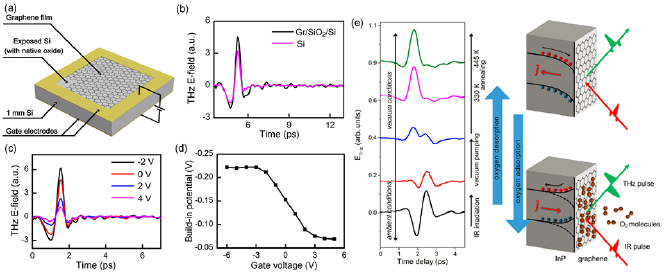
THz radiation from graphene/SiO2/Si heterostructure has been enhanced effectively compared with that from bare Si substrate in the same experimental condition as shown in figures 8(a) and (b) [118]. This enhancement is ascribed to the photocarriers in the interface layer as the pump fluence is insufficient to induce THz radiation from graphene. Since the inversion symmetry of Si is broken by the interface depletion field with a built-in potential φd, the effective second-order nonlinear susceptibility of the interface region is expressed as [58]:

where χ(3) is the third-order nonlinear susceptibility, and EDC is the electric depletion field, which varies along the penetration depth of the pump beam. Thus, the nonlinear process induced by interface depletion field is described as [119]:
Figure 8. (a) Schematic of a graphene/SiO2/Si heterostructure. (b) Enhanced THz radiation from graphene/SiO2/Si compared with that from bare Si substrate. (c) Active THz radiation from graphene/SiO2/Si under different gate voltage Vg. (d) Evaluated interface built-in potential as a function of Vg. (e) Left: oxygen adsorption and desorption dynamics in graphene/InP heterostructure by THz emission spectroscopy. Right: the photoexcited current flows towards the surface of InP due to the surface depletion field modification via O2 adsorption. After removing adsorbates by vaccum pumping and annealing processes, the photoexcited current flows towards the substrate. (a)–(d) Reprinted with permission from [118]. Copyright 2018 American Chemical Society. (e) Reproduced from [123]. CC BY 4.0.
Download figure:
Standard image High-resolution image
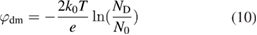
This is the nonlinear polarization from electric field induced optical rectification (EFIOR), hence the emitting THz radiation is proportional to φd. Such interface potential can be tuned by a gate voltage (Vg) to induce an active THz emission, as shown in figure 8(c). As Vg tuning from 6 V to −6 V, the THz radiation as well as φd present saturation under −3 V, and the saturation interface potential is calculated as −0.22 V based on [120]:
where temperature is T = 300 K, N0 and ND are the intrinsic carrier concentration and doping concentration, respectively. On the basis of the relation between the saturation φdm and the THz amplitude, φd as a function of Vg can be extracted (figure 8(d)) according to the THz radiation contribution from pure EFIOR effect. Therefore, this active THz emission enables evaluation of interface built-in potential, which is directly related to carrier distributions, dynamics and band bending, and further determines the performance of mixed-dimensional vdW heterostructure-based devices.
The Fermi level of graphene is sensitive to the external environmental influence such as gas molecule adsorption/desorption and surface/interface processing, and thus the electric and optical properties of graphene-based heterostructures could be influenced by the surface perturbations. Tonouchi et al utilized THz emission spectroscopy as a quantitative and nondestructive measurement tool to probe the gas molecule adsorption/desorption dynamics in graphene-based mixed-dimensional heterostructures. They observed that the THz radiation from graphene-coated InP is related to the adsorbed oxygen (O2) induced localized electric dipoles, which further cause band structure modification in the surface depletion layer of InP [121]. While at graphene/InAs interface, O2 adsorption/desorption showed negligible impact on the THz emission, which was mainly generated by transient diffusion photocurrent [122]. Moreover, they also realized the evaluation of adsorption energy of O2 molecules on graphene- and WS2-based heterostructures due to thermal desorption [123]. As adsorption energy embodies the interaction strength between adsorbates and 2D materials, it is important yet conflicting due to the lack of proper approximation functions to describe dispersion forces [124, 125]. As shown in figure 8(e), take graphene/InP as an example, the generated THz radiation exhibit bipolar waveform at the onset of fs excitation. O2 molecules are adsorbed on the graphene surface and the transient photocurrent flows towards the InP surface. After vacuum pumping, the significant desorption of O2 results in the decreasing of adsorbate concentration and thus influences the photocurrent in InP, which makes the THz signal evolve into a unipolar waveform with a peak at ~2 ps. After further adsorbate removal by annealing, the photocurrent flows towards InP bulk and the resulting THz radiation of graphene/InP is similar to that of bare InP. During this process, the THz radiation contribution of localized electric dipoles induced by O2 adsorbates can be obtained by the variation of THz radiation [123]:

where the subscripts 1 and 2 denote the states without and with O2 adsorbates, respectively. The electric field Edipole is directly related to the adsorbate concentration Nad. Based on this concentration and its dependence on annealing temperature, the adsorption energy of O2 molecules on graphene is estimated as ~0.15 eV. Regarding the adsorption/desorption dynamics, THz emission spectroscopy is not only a direct and contactless tool for molecular surface/interface science, but also facilitates the development of gas sensor devices.
4. Perspective
In this review paper, we summarize the recent progresses on THz emission spectroscopy as a surface/interface characterization tool for advanced materials including graphene, TMDs, topological insulators, hybrid perovskites, and mixed-dimensional heterostructures. THz emission spectroscopy provides rich information such as amplitude, phase, polarization, and polarity of both real and virtual currents in a noninvasive and sensitive way. Thus, THz emission spectroscopy is an interdisciplinary field connecting with the optical physics and condensed matter physics. It could also fertilize the quantum physics such as the superconducting current, valley current and spin current analysis as well as the optic physical analysis in the nanoscale. Expanding this surface/interface THz emission spectroscopy for nanoscale THz spectroscopy [126] is also a very promising research subject for both high-resolution imaging and ultrafast carrier dynamics of bio-chemical molecules and nanoscale materials. Recently, nanoscale THz spectroscopy enables broadband THz emission from a 10 nm scale nanojunction [127], simultaneous 10 nm spatial resolution, and 10 fs temporal resolution [128]. Such spectroscopic technology not only facilitates the understanding of fundamental physics such as electromagnetic field mapping [129], nanoscale phase transition [130], near-field plasmonic coupling [131] etc, but also opens up a wealth of new opportunities for biomedical applications spanning from biomolecules to cells and tissues [132].
However, THz surface/interface emission spectroscopy is far from maturity and needs to be further explored. Firstly, quantitative evaluations of the nonlinear susceptibility values via THz emission spectroscopy are still underdeveloped. This could require a consensus on which analytic method is the most appropriate and precise for extracting the values of nonlinear susceptibility terms via THz emission spectroscopy. It is useful to measure various traditional and advanced materials, and compare the evaluated nonlinear susceptibility values with that from second harmonic generation spectroscopy or from first-principle calculations. Secondly, the procedures of portraying transient photocurrent via THz emission spectroscopy are complicated compared with the direct measurement in photocurrent measurement. Further efforts are required to establish response function models of various detection systems, which will effectively optimize the data processing process and facilitate the accuracy of ultrafast photocurrent extraction. Thirdly, the underlying physical mechanisms of THz radiation for advanced materials are different from traditional materials, and usually more than two mechanisms contribute to THz radiation. How to distinguish these mechanisms is important for the characterization of surface and interface properties of materials. Therefore, theoretical analysis as well as numerical simulation is needed to confirm the THz radiation mechanism. Finally, the light–matter interaction and the consequent THz conversion efficiencies of advanced materials need to be improved. Structural and morphology optimization such as heterostructure, local plasmon enhancement, layer stacking etc, as well as external field modulation including electric, magnetic, or optical fields give rise to the prospects of compact and ultrathin THz sources based on advanced materials.
Acknowledgments
This work was supported by National Natural Science Foundation of China (Nos. 11774288, 11374240), Natural Science Foundation of Shaanxi Province (2017KCT-01) and Excellent Doctoral Dissertation Training Project of Northwest University (YYB17005).