

Abstract
First-principles calculations are employed for the study of the band offsets of AlxGa1−xN alloys, taking into account their composition and atomic configuration. Specifically, the band offsets are obtained using PBE, PBEsol, Heyd, Scuseria, and Ernzerhof (HSE), and modified Becke–Johnson calculations, comparing the results and discussing the advantages and disadvantages of each functional. The band alignments are performed using the branch point energies of the materials as their common reference level. HSE calculations predict a valence band offset of 0.9 eV between GaN and AlN. Regarding the alloys, a conduction band edge bowing parameter of 0.55 eV and a practically zero bowing for the valence band edge is predicted on average. The different atomic configurations affect mainly the valence band edges, where deviations from linearity by more than 0.1 eV are observed.
Export citation and abstract BibTeX RIS
1. Introduction
Group III-nitride semiconductors have demonstrated their technological importance in various applications such as optoelectronics [1, 2], power electronics [3], and photovoltaics [4]. In particular, wurtzite AlxGa1−xN alloys, hereafter called AlGaN for the sake of brevity, feature a wide range of band gaps ranging from 3.4 to 6.2 eV [5] for pure GaN and AlN, respectively, spanning the ultraviolet (UV) and deep UV spectrum. Typical examples of applications in this spectrum involve free space communications, identification of biochemical agents, counterfeit detection, disinfection, and medical diagnostics.
In general, a miscibility gap is observed in group III-nitride mixed crystals in temperatures well above growth temperature [6, 7]. Specifically, phase separation has been observed in InGaN and InAlN alloys in a wide range of compositions [8–15], while the same has been observed in the case of BGaN and BAlN as well, where the boron incorporation is typically less than 3% [15–18]. The spinodal decomposition occurring in the above mentioned cases acts as a strain relief mechanism driven by the internal strain due to the excessive lattice mismatch caused by the presence of indium or boron. AlGaN, on the other hand, is an exception in III–V semiconductors due to the relatively small lattice mismatch between GaN and AlN. The critical temperature for the appearance of the miscibility gap in the case of the AlGaN system has been shown to be much lower than the typical growth temperatures of this material [15, 19]. Hence, excellent solubility is achievable for this system at any composition.
Although pure GaN and AlN have been investigated fairly extensively, the electronic properties of the alloys pose a greater challenge due to the plethora of different atomic configurations and their effect on the properties of the material. Therefore, many discrepancies appear in the reported results for wurtzite AlGaN alloys. For instance, the reported values for the band gap bowing parameter range from −0.8 (upward bowing) to +2.6 eV (downward bowing) [20–31], even though the early findings of an upward bowing have not been reproduced [26, 28]. Furthermore, experimentally measured values for the valence band offset between GaN and AlN range from 0.15 to 1.4 eV [32–35], while theoretical calculations estimate the valence band offset between 0.34 and 1.6 eV [36–47].
The technological importance of AlGaN requires the comprehensive investigation of the electronic properties of this system. However, such an investigation imposes certain challenges from a theoretical point of view. Typical theoretical approaches for the investigation of alloys include the virtual crystal approximation (VCA) [48] and the coherent potential approximation (CPA) [49]. In the VCA, a virtual atom is employed, for which the potential is averaged based on the ionic weights of the atoms in the corresponding alloy, while in the CPA the alloy is replaced by an ordered effective medium where the configurational averaged properties of the real system are calculated using the Green's functions formalism. Even though these methods are computationally inexpensive and have been used extensively in various systems, both of them rely on an averaging scheme and are unable to capture the effects of the various atomic configurations on the properties of the alloys.
It is the aim of this work to investigate the band offsets of the wurtzite AlGaN system over the whole composition range, elucidating the effects of the various atomic configurations by first-principles calculations. Specifically, we employ both standard and hybrid density functional theory (DFT) [50, 51] calculations, including different commonly used functionals in order to compare the results. Furthermore, a discussion is provided aiming to present the advantages and disadvantages of each approach and develop a methodology for the treatment of the band offsets of alloy systems by considering their atomic configurations explicitly.
The manuscript is organized as follows. In the following section (section 2) we describe the method and the details of the calculations. Section 3 presents the results of our calculations, followed by a discussion on the implications of the results and a comparison with the available data in literature in section 4. Finally, section 5 summarizes and concludes the manuscript.
2. Method
Both standard DFT and hybrid functional calculations were employed using the Vienna ab-initio simulation package (VASP) [52]. Specifically, the standard DFT approach refers to calculations with the PBE [53, 54] and PBEsol [55] generalized gradient approximation (GGA) functionals. Hybrid functional calculations were performed in the parameterization by Heyd, Scuseria, and Ernzerhof (HSE) [56, 57]. Finally, the Tran–Blaha modified Becke–Johnson (mBJ) [58, 59] meta-GGA functional was also employed and compared to the computationally more expensive HSE calculations.
The alloys were studied considering the exhaustive set of wurtzite atomic configurations in supercells of up to 16 atoms generated by the ATAT code [60, 61]. A total number of 401 distinct atomic configurations in 13 different compositions including the binaries were employed. For consistency purposes, Γ-centered k-point meshes with a density of at least 1000 k points per reciprocal atom were used for all the supercells throughout the calculations. Furthermore, all the calculations were spin polarized with an energy cutoff of 500 eV for the plane-wave basis set, while the gallium 3d electrons were treated as valence electrons. The supercells were optimized using both atomic and volume relaxations, with a force criterion of 10−3 and 0.02 eV Å−1 for the standard DFT and hybrid functional calculations, respectively. Specifically, PBE, PBEsol, and HSE results correspond to structures optimized with their corresponding functional, while mBJ results correspond to structures optimized with the PBEsol functional.
Although standard DFT calculations typically underestimate the band gap of semiconductors significantly [62], they remain popular due to the considerably lower computational cost compared to other approaches such as hybrid functional or GW calculations. An improved description of the band gap at almost the same cost as standard DFT calculations arises from the mBJ [58, 59] meta-GGA functional, which yields band gaps with an accuracy similar to hybrid functional or GW calculations and in very good agreement with experimental data [63, 64]. The mBJ potential by Tran and Blaha [58] is a modification to the Becke–Johnson (BJ) [59] potential and is given by

where  is the Becke–Roussel (BR) [65] potential,
  is the electron density, and
  is the kinetic energy density. For c = 1 the original BJ [59] potential is recovered. Parameter c in equation (1) is defined as

where α and β are empirically determined parameters and Ω is the volume of the supercell. The typical values of α = −0.012 (dimensionless) and β = 1.023 bohr1/2 are obtained by minimizing the mean absolute relative error for the band gap of the solids listed in table 1 of reference [58]. In general, the optimal value copt which yields perfect agreement with the experimental band gaps lies in the range of 1.1–1.3 and 1.4–1.7 for small and large band gap materials [58], respectively and is typically different from the self-consistent value obtained by equation (2).
The experimental band gaps of GaN and AlN are reproduced with HSE calculations using a Hartree–Fock (HF) mixing parameter of 0.28 and 0.32, respectively. Regarding the alloys, a linear interpolation between the values of 0.28 and 0.32 was employed for the study of the alloys, as described elsewhere [36]. Similar to the HSE calculations, a single c parameter of the mBJ potential is not able to reproduce the band gaps of both GaN and AlN at the same time. In the case of mBJ calculations though, there are a few different ways to treat parameter c. First, parameter c can be determined self-consistently by the electron density as shown in equation (2), where α and β are empirical parameters. An other way is to set parameter c to a value that reproduces the band gap of the given material, in which case it is usually referred to as optimal c. Finally, the last approach is to set a species-specific ci parameter. In this case, the mBJ potential at point r is calculated using the parameter ci belonging to the atomic species which is nearest to the position r.
In general, the electronic properties of alloys, such as the band gap and the band offsets, change in a non-linear fashion with respect to the composition. In such cases, a quadratic behavior is typically assumed. Therefore, a quantity Q of a compound A1−xBx can be expressed as

where QA and QB refer to the given quantity of the pure constituents A and B, respectively. The factor b is commonly called the bowing parameter of the given quantity and determines the degree of nonlinearity. Positive values of the bowing parameter result in convex behavior (downward bowing), while negative values indicate concave behavior(upward bowing). Equation (3) can be applied to the conduction and valence band edges independently, giving rise to the bowing parameters bc and bv, respectively. Furthermore, the total bowing parameter of the band gap can be expressed in terms of bc and bv by the relationship bg = bc − bv. In this work, the constituents A and B refer to pure GaN and AlN, respectively.
Various methods for aligning the band edges of different materials are available through first-principles calculations. Some of the most commonly used methods are the alignment with respect to the vacuum level following Shockley–Anderson's electron affinity rule [66–68] and the alignment using the heterostructure approach [69, 70]. These methods use the average electrostatic potential along a certain direction as a reference level by employing a supercell of specific orientation. Moses et al [37] have shown that the average electrostatic potential is sensitive to the stoichiometry of the alloy in each layer perpendicular to the chosen direction in which the electrostatic potential is averaged. This finding imposes an insurmountable challenge for alloy systems, since very few atomic configurations fulfill this condition. The conditions become even more stringent in the case of wurtzite AlGaN because non-polar directions should be used in order to avoid polarization fields that affect the alignment. Therefore, the above mentioned techniques are unpractical for a comprehensive study of the band offsets in alloy systems.
A different approach which is more suitable for alloy systems is the alignment with respect to the branch point energy of each material [71, 72]. The branch point energy or charge neutrality level of each material is given by [71]

where Nk refers to the total number of k points on which the summation is performed. A number of NCB and NVB of the lowest and uppermost conduction and valence bands, respectively, are included in the calculation of the EBP. Furthermore,  and
and  refer to the energy eigenvalues of the chosen conduction and valence bands. Since the number of bands increases with the number of atoms in the supercell, for consistency purposes, two conduction and four valence bands per primitive cell were employed4 in the calculation of the branch point energy in the alloy supercells. Once EBP is determined by equation (4), the valence band maximum (VBM) and conduction band minimum (CBM) obtained by the bulk calculation may be referenced to the branch point energy as
  and
and  , respectively. As a result, the band edges of different structures can be aligned using
  and
and  .
.
At this point it is also useful to mention that not all the 401 configurations employed in this study are equally likely to occur in reality. Furthermore, the present work does not examine the occurrence likelihood of each configuration. Instead, the aim is to rely on a reasonably large number of configurations in order to infer the possible variation of the band gaps and band offsets of the alloys due to the atomic configuration. A more detailed discussion about the formation energies of these structures, and the fact that they alone are not sufficient to provide a definite answer for the occurrence frequency of each configuration is provided elsewhere [36].
3. Results
The band gaps were obtained using the PBE and PBEsol GGA functionals, the HSE hybrid functional, and the mBJ meta-GGA functional using three different approaches for the determination of parameter c. Figure 1 shows the band gaps obtained by the PBE, PBEsol, and HSE calculations. As expected, the GGA functionals underestimate the band gaps of the binaries and the alloys. Specifically, the values of 1.72 and 1.91 eV were calculated for the band gap of GaN using PBE and PBEsol, respectively. In the case of AlN the band gaps from PBE and PBEsol were 4.07 and 4.12 eV, respectively. The minor differences between the PBE and PBEsol results are attributed to the fact that the latter is optimized for solid calculations and that these two GGA functionals predict slightly different lattice constants. On the other hand, the HSE functional is able to reproduce the correct experimental band gaps for the pure GaN and AlN using an appropriate HF mixing parameter and, therefore, it provides a better description of the band gaps of the alloys. Nonetheless, standard DFT calculations are in good qualitative agreement with the more expensive HSE calculations, except for the systematic underestimation of the band gap of each structure.
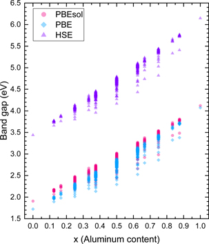
Figure 1. The band gaps of the alloys obtained by HSE, PBE, and PBEsol calculations.
Download figure:
Standard image High-resolution imageThe mBJ calculations were performed following the three different methods discussed earlier for the determination of parameter c. The atomic structures were optimized using the PBEsol functional before performing the calculation with the mBJ potential for the determination of the band gap. In the case of the self-consistent determination of c, its value is obtained by equation (2) using the charge density and the default values of α and β. The values of c = 1.335 and c = 1.297 with corresponding band gaps of 3.00 and 5.49 eV were obtained for GaN and AlN, respectively. This is already a significant improvement over the standard DFT approach at only marginally higher computational cost. The band gaps of all the atomic configurations obtained with a self-consistent parameter c are shown as blue triangles in figure 2. These values are still smaller than the experimental data and a larger c is necessary to achieve a better agreement.

Figure 2. The mBJ values of the band gaps obtained by a self-consistent, optimal, and species-specific c parameter, compared to the values obtained by HSE calculations.
Download figure:
Standard image High-resolution imageA much better agreement between the mBJ and HSE calculations is observed in the other two cases. Regarding the case of an optimal c parameter, the values of  and
and  yield values of 3.44 and 6.15 eV for the band gaps of GaN and AlN, respectively. Similar to the HSE calculations, the value of c for the alloys was varied linearly between the values of the binaries. The results of this approach versus the HSE band gaps are shown as green circles in figure 2. The last case refers to the use of a species-specific parameter ci. A parametric study of ci was performed with respect to the band gaps of pure GaN and AlN, revealing that the results are mainly affected by cGa and cAl. The values of cGa = 1.50, cAl = 1.54, and cN = 1.47 were obtained by the best fit to the parametric study and were eventually used in the alloy calculations. The results for the species-specific c parameter are presented in figure 2 with purple diamonds.
The alignment of the band edges of alloys of different compositions and atomic configurations was facilitated by the use of their branch point energies as the common reference level. The advantage of this approach is that it does not require the use of an interfacial supercell, whether it is with vacuum or a different material, where various stringent conditions need to be met. Instead, the bulk supercell of each structure may be used directly. Therefore, all the different atomic configurations can be investigated without exception. Naturally, the investigation of the band offsets requires the accurate description of the band gaps. In that respect, PBE, PBEsol, and mBJ calculations with a self-consistent c parameter yield band gaps that are typically smaller than the experimental data. Therefore, these calculations might not be suitable for the investigation of the band offsets, unless an ad hoc correction is applied in order to account for the underestimation of the band gap. Approaches such as HSE and mBJ calculations with variable mixing parameters provide a better description of the band gaps. Consequently, these methods appear to be more suitable for the study of the band offsets.
The results of the band offsets obtained by HSE calculations, as well as mBJ calculations with an optimal and a species-specific c parameter are presented in figures 3(a)–(c), respectively. The VBM of GaN is set to zero in all cases for convenience. The mean value and the standard deviation of the conduction and valence band edges at each composition are shown with diamond markers and shaded areas, respectively. The solid lines represent the least squares fit of equation (3) for the valence and conduction band edges separately. In the case of the HSE calculations, shown in figure 3(a), the valence band offset between GaN and AlN is 0.90 eV, while in the mBJ calculations, shown in figures 3(b) and (c), the valence band offset is 0.93 eV. The conduction band offset between GaN and AlN is 1.81 and 1.77 eV obtained by HSE and mBJ calculations, respectively. The mBJ results using the self-consistent value of the c parameter yield a valence and conduction band offset between the binaries of 0.80 and 1.69 eV, respectively. Consequently, a good agreement between HSE and mBJ is observed for the band offsets of the pure binaries. The results are listed in table 1.
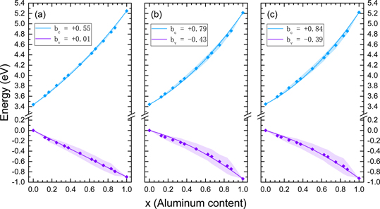
Figure 3. The band offsets of the alloys obtained by (a) HSE calculations, as well as mBJ calculations with (b) an optimal and (c) a species-specific c parameter. The legends indicate the bowing parameter of the valence and conduction band edges. The valence band edge of GaN is set to 0 eV for convenience.
Download figure:
Standard image High-resolution imageTable 1. The band gaps for pure GaN and AlN, the valence and conduction band bowing parameters for the alloys, and the valence (ΔEv) and conduction (ΔEc) band offsets between the binaries, obtained by the four different functionals. The units of all the values are in eV.
| mBJ | ||||||
|---|---|---|---|---|---|---|
| Property | HSE | PBE | PBEsol | optimal c | Species-specific c | Self-consistent c |
 | 3.44 | 1.72 | 1.91 | 3.44 | 3.45 | 3.00 |
 | 6.15 | 4.07 | 4.12 | 6.15 | 6.15 | 5.49 |
| bv | +0.01 | −0.02 | +0.04 | −0.43 | −0.39 | −0.28 |
| bc | +0.55 | +0.58 | +0.55 | +0.79 | +0.84 | +0.75 |
| ΔEv | 0.90 | 0.77 | 0.73 | 0.93 | 0.93 | 0.80 |
| ΔEc | 1.81 | 1.58 | 1.48 | 1.77 | 1.77 | 1.69 |
The striking difference between the two approaches lies in the results of the alloys. The mean values of the valence band offsets obtained by HSE calculations yield a valence band bowing of 0.01 eV, indicating a practically linear change of the valence band offsets throughout the whole composition range. The conduction band bowing parameter was 0.55 eV according to the HSE calculations. On the other hand, mBJ calculations yield a valence band bowing of −0.43 and −0.39 eV for an optimal and a species-specific c parameter, respectively. This negative bowing can also be seen by the concave behavior of the valence band offsets in figures 3(b) and (c). Furthermore, the conduction band bowings are 0.79 and 0.84 eV resulting in a total band gap bowing of 1.22 and 1.23 eV, respectively. Additionally, the mBJ calculations with a self-consistent c parameter yield the values of −0.28 and 0.75 eV for the valence and conduction band bowing parameters, respectively. Apparently, the total band gap bowing parameter obtained by the mBJ calculations is much larger compared to the HSE calculations. This is not surprising, since it was evident from figure 2 that even though HSE and mBJ calculations agree on the values of the binaries, the latter systematically underestimate the band gaps of the alloys.
It was mentioned earlier that standard DFT faces certain limitations on the description of the band offsets due to the underestimation of the band gap. This is true when one considers the full picture where both the band edges and the band gaps should be described properly. However, one might examine the alignment of the conduction and valence band edges separately, focusing only on their corresponding offsets and bowing parameters without considering the correct value of the band gap. Figure 4 shows the band offsets of the alloys, obtained by the PBE and PBEsol functionals. Although the band gaps are significantly smaller than the experimental values, the results are in good agreement with HSE calculations. Specifically, the valence band offset between GaN and AlN obtained by PBE and PBEsol calculations is 0.77 and 0.73 eV, respectively. Also, the valence band bowing parameter is −0.02 and 0.04 eV. Regarding the alignment of the conduction band edges, PBE and PBEsol calculations yield an offset of 1.58 and 1.48 eV between GaN and AlN, with corresponding conduction band bowing parameter of 0.58 and 0.55 eV. Therefore, the bowing parameters obtained by standard DFT calculations are in excellent agreement with the ones obtained by HSE calculations. Table 1 summarizes the results.

Figure 4. The band offsets of the alloys obtained by PBE and PBEsol calculations. The legends indicate the bowing parameter of the valence and conduction band edges. The valence band edge of GaN is set to 0 eV for convenience.
Download figure:
Standard image High-resolution imageA common characteristic which is captured by all the different calculations is the fact that the valence band edges of the alloys exhibit larger standard deviations compared to the conduction band edges. The variations of the valence band edges are caused by the different atomic configurations. On the other hand, the conduction band edges are less sensitive to the various atomic configurations. This result can be discussed on the basis of the information derived by combining figures 1 and 3(a). The results presented in figure 1 indicate that the total bowing parameter takes non-negative values. Specifically, there are structures whose band gap lies on the straight line connecting the binaries yielding zero bowing and others that indicate a total bowing parameter that reaches large positive values. This can be explained in terms of the results presented in figure 3(a) regarding the valence band edges. Although a zero valence band bowing is calculated by the mean values of the valence band edges, the large deviations allow for large positive or negative values of the valence band bowing parameter. Hence, a large downward deviation of the valence band edges (bv > 0) counteracts the conduction band bowing, which is less sensitive in changes due to the various atomic configurations, yielding a total zero bowing for the band gap. Similarly, an upward deviation for the valence band edges (bv < 0), further increases the total bowing parameter of the band gap.
A closer inspection of the atomic configurations that cause large deviations from linearity for the valence band edges in different compositions reveals certain trends. In general, structures where the cations are homogeneously mixed, were found to exhibit downward deviation from linearity. On the other hand, structures where the cations are poorly mixed, such as superlattices, exhibited an upward deviation of their valence band edges. This result is consistent with a previous work [36] for the AlGaN system as well, where the alignment with respect to the vacuum level was employed to study the band offsets between the binaries and Al0.5Ga0.5N alloys.
4. Discussion
The main goal of this work is to employ DFT calculations and demonstrate different approaches for the investigation of the electronic properties of alloy systems. In this effort, standard DFT, hybrid functional, and mBJ calculations were performed. In the case of HSE and mBJ calculations a variable HF mixing parameter and c parameter were utilized, respectively. Therefore, it is essential to discuss the use of a variable mixing parameter and its effects on different properties of the material before commenting on the results of this work. The mBJ calculations with a variable c parameter are similar to HSE calculations in many respects, since the mBJ potential can be viewed as a kind of hybrid potential where the amount of exact exchange is given by c [58]. Therefore, the term mixing parameter will be used interchangeably for both functionals in the discussion that follows.
Although the thermodynamic properties of the AlGaN alloys are beyond the scope of this work, it is worth mentioning the effects of a variable mixing parameter on these properties for completeness. These properties rely on the comparison of the total energies of different structures. The mBJ functional is a potential-only functional. Therefore, the calculations are not self-consistent with respect to the total energy and the total energies obtained by this functional cannot be used for the study of thermodynamic properties, regardless of the value of c. Instead, this functional is intended only for the description of the electronic properties of the system. Regarding the HSE calculations, the mixing parameter affects the total energy and, consequently, a comparison of the total energies of different alloys with the total energies of the pure binaries in order to obtain their formation enthalpies would be detrimental when a variable mixing parameter is used. A different functional such as PBE or HSE with constant mixing parameter for all the involved structures would be more suitable in this case.
The effects of the mixing parameter on the electronic properties of the system depend on the specific property under investigation. For instance, the band gaps are obtained as the difference of the eigenvalues of the CBM and the VBM. Even though the mixing parameter of both HSE and mBJ significantly affects these eigenvalues the band gap is an inherent property of each material and is independent of the band gap of different structures. Therefore, an optimized mixing parameter may be utilized in order to describe the band gap of each structure independently. Contrary to the band gaps, the band offsets are given as a relative quantity among the structures. Regardless of the method of choice for obtaining the band offsets, the band edges of each structure are aligned with respect to a chosen reference level. Therefore, it is essential to examine the effect of a variable mixing parameter on the reference level of choice in order to verify the validity of the results.
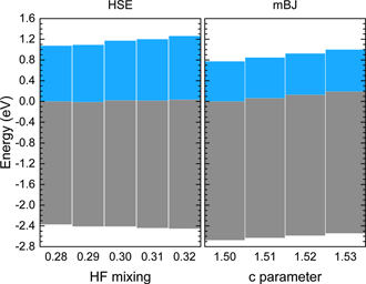
Using the Shockley–Anderson's electron affinity rule [66–68] the alignment occurs with respect to the vacuum level. In a previous work [36] it was shown that a variable mixing parameter in HSE calculations does not affect the reference level in the AlGaN system using this method of alignment. Furthermore, in the heterostructure approach [69, 70] the band edges are aligned with respect to the average electrostatic potential at each side of the interface between the two materials. Alkauskas et al [70] showed that varying the mixing parameter in HSE calculations only marginally affected the reference levels and therefore a variable mixing parameter was justified in the case of the heterostructure method as well. In our case, the branch point energies of the alloys were used as the common reference level for the alignment of their band edges. The mixing parameter of the HSE calculations ranges between 0.28 and 0.32. In this range, the branch point energy of pure GaN, AlN, and the alloy structures was found to remain practically constant versus the HF mixing parameter. Specifically, the maximum deviation of the branch point energy of each structure was less than 0.04 eV, while in most cases the deviation was of the order of 0.02 eV. In the case of the mBJ calculations, the c parameter was found to greatly affect the branch point reference level by more than 0.17 eV. Figure 5 demonstrates the effect of a variable mixing parameter in HSE and mBJ calculations for the case of GaN by showing the band gap and the branch point energy in a range of mixing parameters that were relevant for the calculations in both schemes. The branch point energy obtained by the smallest mixing parameter in each scheme is set to zero for convenience.
Figure 5. The effect of a variable Hartree–Fock mixing (HSE) and c (mBJ) parameter on the branch point energy of GaN. The first branch point energy of each method is set to 0 eV for convenience. The blue and gray boxes indicate the difference from the branch point energy to the conduction and valence band edge, respectively.
Download figure:
Standard image High-resolution image
As mentioned above, HSE calculations with a varying mixing parameter maintain a constant reference level and are suitable both for the study of band gaps and the band offsets. On the contrary, even though mBJ calculations improve the description of the band gaps compared to standard DFT calculations, the effect of a varying mixing parameter is detrimental since the reference level varies significantly, hence making this functional unsuitable for the band offsets. Additionally, one of the known [73] shortcomings of the mBJ functional is its limited success on the description of the effective masses, which is directly related to the accurate determination of the energy eigenvalues in the Brillouin zone. However, since a good description of the eigenvalues is essential for the determination of the branch point energy, the use of the mBJ potential is further exacerbated5.
A comparison of the calculated and experimental band gaps and band offsets of GaN and AlN is possible due to the uniqueness of these structures. However, in the case of alloys, the comparison is not straightforward due to the plethora of different atomic configurations. Therefore, other macroscopic indicators such as the bowing parameter should be employed in order to facilitate a comparison with experimental data. The experimental values for the band gap bowing parameter of the AlGaN system range from −0.8 eV to +2.6 eV [21–31]. However, the early reports of an upward (negative) bowing have not been reproduced [26, 28]. Figure 1 indicates a non-negative bowing parameter supporting the experimental results. A detailed comparison of the effect of the different atomic configurations of the alloys on the bowing parameter was presented in a previous work [36], where it was shown that the PBE and HSE calculations yield the same total bowing parameter. In the case of mBJ calculations, although the band gaps of GaN and AlN are in excellent agreement with experimental data, the alloys exhibit a larger bowing parameter than HSE, as shown in figure 2.
The band offsets obtained in the present work refer to the natural or unstrained band offsets. Therefore, the results could be compared to results obtained by the ionization potentials (IP) and electron affinities (EA) of unstrained materials. The IP is defined as the VBM referenced to the vacuum level, while the EA corresponds to the CBM referenced to the vacuum level. The experimental values of the EA of GaN range from 2.6 to 3.5 eV [74–77]. In the case of AlN, the experimental values of the EA range from 0 to 1.9 eV [76, 78]. Therefore, the conduction band offset between GaN and AlN ranges from 0.7 to 3.5 eV according to the experimental data. It should be noted that the wide discrepancy of the experimental values is caused by the challenging task to accurately determine the EA due to surface contamination and oxidation of the samples. Our results indicate a conduction band offset of 1.81 eV, which is in reasonable agreement with the experimental data. Furthermore, the branch point energies of GaN and AlN were found to be 2.37 and 3.27 eV above the VBM, respectively, according to the HSE calculations. Hence, the valence band offset between the binaries is 0.9 eV. These results are in excellent agreement with the results obtained by Schleife et al [71], where they calculated branch point energies of 2.37 and 3.33 eV for GaN and AlN, respectively, yielding a valence band offset of 0.96 eV.
Finally, it should be noted that the methods of alignment with respect to the vacuum level or the branch point energy should in principle yield similar results since they both refer to the natural band offset. Previous [36, 37] calculations employing the vacuum level as the reference level reported a valence band offset between GaN and AlN of 0.40–0.46 eV.These values are nearly half the ones reported here and elsewhere [71] by the method of alignment with respect to the branch point energies. Evidently, even though both methods yield values that are within the range of experimental results and are consistent with other similar calculations, there seems to be a discrepancy. A reasonable explanation for this discrepancy is not available. Nevertheless, both methods agree to the fact that the various atomic configurations mainly affect the valence band offsets rather than the conduction band offsets. This may be seen in figures 3 and 4, where the standard deviations of the valence band edges of each composition are much larger compared to the conduction band edges. The deviations arise from the different atomic configurations of the alloys.
The above mentioned effect was previously demonstrated [36] using two different kinds of structures and only for Al0.5Ga0.5N, due to the stringent requirements of the vacuum level approach regarding the atomic configurations. The first structure was representative of atomic configurations where the cations are poorly mixed, such as superlattices, while the second structure represented the cases where the cations are homogeneously mixed. It was found that in the former case an upward deviation from linearity appears for the valence band offsets, while a downward deviation was observed for the latter. In this work, the chosen method for the alignment of the band edges allows for the inclusion of all the different structures in all compositions without exceptions. Therefore, a much larger sample of atomic configurations can be examined. The results obtained by the comprehensive study among all the different structures are in excellent agreement with the previously reported data. Combining the information provided in figures 1–3, the variation of the band gaps arises mainly by the different position of the valence band edges. Specifically, alloys with a homogeneous distribution of cations yield larger band gaps and a downward valence band bowing, while the opposite applies for poorly mixed alloys, such as superlattices.
5. Conclusion
The band offsets of AlGaN alloys were investigated employing different levels of theory. Specifically, standard DFT, hybrid functional and mBJ calculations were performed on all the possible atomic configurations generated by supercells of up to 16 atoms in order to investigate the effect of the various atomic configurations of the alloys on their band offsets. The band alignment relied on the branch point energies of the alloys as their common reference level, allowing for the investigation of all the structures at a small computational cost.
Standard DFT calculations underestimated the band gap of the binaries and the alloys but the band gap bowing parameter was in excellent agreement with HSE calculations. Regarding the mBJ calculations, excellent agreement with the HSE calculations was observed only for pure GaN and AlN. The band gaps of the alloys obtained by mBJ calculations exhibited smaller values compared to HSE calculations, yielding an overall larger bowing parameter.
The valence band offset between GaN and AlN was 0.90 and 0.93 eV, obtained by HSE and mBJ calculations, respectively, while PBE and PBEsol calculations predicted a value of 0.77 and 0.73 eV. Therefore, the band offset between GaN and AlN obtained by mBJ calculations was in better agreement with HSE calculations. Nevertheless, mBJ calculations failed to yield the same level of agreement for the alloys. Instead, standard DFT was in excellent agreement with HSE calculations for the valence and conduction band bowing parameters of the alloys, regardless of the poorer description of the band gaps. Overall, the mean values of the valence band edges were found to change linearly versus the composition of the alloy while a conduction band offset bowing of 0.55 eV was calculated for the composition dependence of the conduction band edges. Nonetheless, it should be noted that a minimal variation of the conduction band edge was observed for the alloys, while a large spread of more than 0.2 eV was observed in the valence band offsets due to the different atomic configurations. Specifically, homogeneous mixing of the cations was found to yield a downward deviation of the valence band offset from linearity, while poorly mixed configurations such as superlattices caused an upward deviation.
Finally, we discussed the effects of a variable mixing parameter in HSE and mBJ calculations on the electronic properties of the materials. Such practice is certainly beneficial for the description of the band gaps but might be detrimental for the band offsets. Thus, the impact of the variable mixing parameter on the reference level used for the band alignment should always be carefully examined. The mBJ calculations were found to be unsuitable for the study of the band offsets of the alloys since the reference level of the band edges was inconsistent versus a variable c parameter. On the contrary, HSE calculations were found suitable both for the description of the band gaps and the band offsets.
Acknowledgments
This work was supported by the US Army Research Laboratory through the Collaborative Research Alliance for Multi-Scale Multidisciplinary Modeling of Electronic Materials (Grant No. W911NF-12-2-0023). The computational resources were provided by the DoD HPC Systems and the 2019 Army Research Office DURIP Award (Grant No. W911NF-19-1-0161).
Footnotes
- 4
For instance, in the 16-atom supercell one would need four times more valence and conduction bands compared to the primitive cell.
- 5
It is important to note that the results for the mBJ functional were not affected by the choice of the PBEsol-relaxed structures. The results were the same as well for the HSE-relaxed structures with appropriately optimized mixing parameters.