

Abstract
Phononic crystals (PnCs) are capable of manipulating the flow of elastic energy through their periodic structures and have emerged as a promising field in the last two decades. Thanks to the advances in microfabrication technologies and developments of multifunctional materials, the engineering of periodic structures moves forward to the nanometer scale. Hence, the relevant frequencies of elastic waves are pushed toward the gigahertz regime where strong photon-phonon interactions trigger the applications of PnCs towards information and communication technologies. In this review, we present the experimental achievements on hypersonic PnCs involving microfabrication technologies to realize the desired structures and characterization of their band structures for unraveling phonon propagation modulation. Some application-oriented research directions are proposed in terms of advances in fabrication and characterization technologies and the development of electro-optomechanical systems.
Export citation and abstract BibTeX RIS

Original content from this work may be used under the terms of the Creative Commons Attribution 4.0 license. Any further distribution of this work must maintain attribution to the author(s) and the title of the work, journal citation and DOI.
1. Introduction
The last two decades witnessed the emergence of one very promising new field in physics, that is the extraordinary ability to mold the flow of (electromagnetic and elastic/acoustic) waves by designing macroscopic materials with periodic physical properties [1–3]. Engineering wave propagation can yield many new phenomena that cannot be achieved by natural materials, such as energy band gap [4], cloaking [5, 6], and negative refraction [7], making those artificially structured materials gain enormous interest from both fundamental and applied science. The concept of wave modulation started with the photonic crystals (PhCs) proposed by Yablonovitch [8] and John [9] in 1987, that is the electromagnetic wave propagation can be manipulated in the systems with periodic variation of the dielectric constant in analogy to the electron propagation in the crystalline solids. One of the most striking features of PhC is the presence of the photonic bandgap which can prevent propagation of light along certain directions when the structure periodicity is in the order of the wavelength of light. Thanks to the rapid developments of (nano-) fabrication technologies, the photonic structure can be designed in one, two, and three dimension and the periodicity spans from nanometer to centimeter [10]. Thus, the light can be controlled over a broad frequency, opening pathways for many applications switched by photons rather than electrons.
Besides photons, another important particle which is able to carry the energy and information is the phonon. As an expression of atomic motion, phonons can be considered as the quantized sound waves that propagate in a medium with a velocity depending on the elastic properties (stiffness and mass) of materials. The significance of phonon is met not only in science but also in everyday life and industry. The frequency of phonons extend over a broad range, from few Hz to dozens THz, where only a narrow range, from 20 Hz to 20 kHz, is audible [11]. The inaudible phonons are crucial in diverse applications based on their frequencies. For instance, at frequencies below the lower limit of human audibility, infrasound possesses a high transmissivity that can get around obstacles with little dissipation, thus, it is used as an important detection technique for the study of seismography [12]. At higher frequencies above the upper audible limit, ultrasound (from 20 kHz to 1 GHz) is a critical tool in imaging and non-destructive testing, hypersound (from 1 GHz to 1 THz) is utilized in the signal processing and acousto-optics devices [13–15]; and the higher frequency (>1 THz) range is responsible for thermal transport and thermal management [16]. Therefore, it would be valuable to realize the modulation of the phonons to a similar degree as those remarkable achievements in manipulating electrons and photons [17].
In 1993, the concept presented for PhCs was theoretically transferred to the phononic crystals (PnCs) by properly varying the elastic properties of structured materials [18, 19]. In principle, gaps and bands can appear in the propagation of acoustic (elastic) waves if the material's elastic properties, elastic moduli and/or density, can be periodically designed [20]. When the wavelength is much longer than the distance between atoms, phonon behaves in a wave-like nature that could be described by classical continuum mechanics [21]. The interference of incident and reflected elastic waves occurs when the wavelength of phonon is comparable to the lattice spacing, giving rise to the appearance of Bragg-like gap (BG) [22]. Besides Bragg scattering, there is another opening mechanism of band gap, that is the so-called hybridization gap (HG) which is associated with the coupling between the propagating wave and local resonances [21, 23]. It should be noted that the local resonance has flat dispersion in contrast to the Bragg resonance that occurs at the gap edge. Accordingly, the local resonance in the phononic structure, rather than its periodicity, determines the HG features. Generally speaking, the bandgaps can be explained by the interference of waves scattered by all periodic units, regardless resonant or not [18, 19, 24]. As the band structure that describes the propagation of phonon is one of the fundamental properties of PnCs, full control of the phonon dispersion relation is the primary objective of PnCs [25].
The spacing of the PnCs structure ranges from macro- to nano-meters depending on the elastic-wave frequency of interest [1]. Since the band structure is scalable with the structure periodicity in the framework of linear elasticity theory, the artificial periodic structures were initially built in the macroscopic scale to manipulate low-frequency phonons (kHz) with large traveling distances [26, 27]. Downscaling the structural dimension to sub-micrometer, high-frequency phonon (GHz) is controllable in a similar manner as that of lower-frequency phonon ignoring dissipation effects. Moreover, high-frequency phonons can strongly interact with photons of comparable wavelength [11], and hence their coupling has received strong attention [28–30]. The field of optomechanics [31] utilized the radiation pressure of light to control the mechanical motion, demonstrating high impact on both applications and fundamental investigations [14, 32, 33]. However, the experimental exploration of PnCs at hypersonic frequencies faced challenges in terms of the micro-structural fabrication and characterization of such high-frequency phonons. The former has been overcome by the rapid progress in nanotechnology [34], especially the methods developed in colloid and polymer science that created versatile novel materials with controlled properties at the microscopic scale [35, 36]. The latter relies on indirect electroacoustic platforms [37–39] and direct Brillouin light spectroscopy (BLS) measurements [40]. It should be noted that the hypersonic phonons describe the elastic waves in the GHz regime, which is different from the hypersonic flow/speed that refers to the flow velocity exceeding five times the sound speed in aerodynamics field. Nevertheless, the thrive advancements in materials science allow to deliberately engineering the phononic band structure of materials in the high-frequency range, thus stimulating experimental and theoretical explorations on the hypersonic PnCs in the last two decades [41–46]. Phonons with frequencies of several THz are responsible for heat transport. These thermal phonons have received lot of interests given their potential heat management applications such as in thermoelectrics and thermal diode. Thermal phonons propagation and thermal transport at nanoscales have been reviewed in several papers in the literatures [47–50], which will be not discussed in this work. On the experimental side, the spectra recorded at THz frequencies and hence wavevectors q using inelastic x-ray scatterings suffer from the low resolution due to the inherent broadening (∼q2) [51].
In this review, we present progress and perspectives along with the fundamental description on the PnCs that are capable to modulate elastic waves at hypersound frequencies. The paper is organized as follows. In section 2, we first summarize the advances in fabrication techniques that are employed to build periodic structures of PnCs with feature size in sub-micrometer scale. In section 3, the fundamental features of the band structure of hypersonic PnCs and the origin of hypersonic phononic bandgaps are described. In section 4, we explore the experimental assessments on the band structure of hypersonic PnCs with periodicity in different dimensions. Finally, in last section 5, we provide some perspectives of fundamental research interests and application-directed research on the hypersonic PnCs.
2. Fabrication of hypersonic PnCs
Fine tailoring of periodic structures is essential for achieving the functionalities of PnCs in practical applications. A high-quality PnC requires the precise control of periodicity while avoiding the generation of random defects [52]. The latter can modify the band structure, and thus may cause a negative impact on the practical performances. At GHz frequencies, the feature size of PnCs is in the sub-micrometer range. This length scale limits the fabrication to a few technologies [34], such as microfabrication, casting, and wet-chemical techniques. For a given PnC, selecting a suitable and efficient fabrication technology is important and is mainly determined by the material properties, geometry of inclusions, and the patterned structures. We summarize next state of the art of the fabrication for one-, two- and three-dimensional PnCs.
2.1. One-dimensional PnCs
1D PnC consists of two or more repetitions of layers along a certain direction. Simple 1D PnCs are composed of a periodic grating coated on a uniform substrate. This pattern-like surface could confine surface acoustic waves (SAW) [21], enabling their applications in signal processing such as interdigitated transducers [53]. Microlithography is a popular approach to create well-defined micro or nanogratings with an aspect ratio of up to 10 [54]. Microlithography, traditionally used in the semiconductor industry, is flexible and versatile technique, and compatible with different strategies necessary to create more complex structures. Together with the deposition process, it can write micropatterns with out-of-plane dimension spanning from few nanometers to hundreds of micrometers [55]. The microlithography utilizes a pre-fabricated mask or reticle as a master to derive the final pattern as shown in figure 1(a). According to the energy being used on the photoresists, photolithography and electron beam lithography (EBL) are the most common top-down techniques for fabrication of structures from bulk to nanosized scale. Unlike the one-step techniques, such as 3D printing, microlithography involves multiple steps as illustrated in figure 1(a). A layer of photoresist on the substrate is shaded by a mask, and then exposed to an ultraviolet (UV) light. The exposed photoresist is chemically modified by the UV light, becoming either soluble (positive) or insoluble (negative). Then the patterned photoresist layer in turn serves as a masking layer in the following etching process that transfers the pattern to the substrate. Dhar et al employed the photolithography method to fabricate 1D grating with a periodicity of a few microns revealing a complete phononic bandgap at a few tenths of a gigahertz [56]. EBL is conceptually similar to photolithography but replaces the light with a beam of focused electrons. Therefore, the resolution is not diffraction-limited common to the optical techniques employed in the photolithography. Moreover, EBL can directly write the patterns on the photoresist without the mask [57] as shown in figure 1(d), but the process is relatively time-consuming and costly as compared to photolithography. Holographic lithography is another technique for drawing regular fined arrays without the use of photomasks. The principle being the same as the holographic technique utilizes the advantage of the interference pattern of the coherent light to build a periodic series of fringes. Via holographic lithography, Li et al fabricated the ultrahigh-aspect-ratio (up to 10) nanogratings with width ranged from 200 nm to 500 nm [54]. Note that the above lithography techniques can be applied to both inorganic and organic materials.
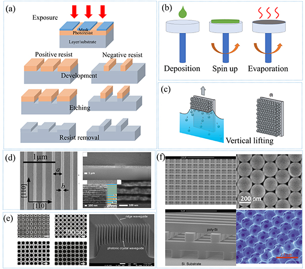
Figure 1. Fabrication techniques and microstructures of PnCs. Schematic of (a) microlithography, (b) spin coating, and (c) vertical lifting processes. Reprinted by permission from Springer Nature Customer Service Centre GmbH: [Springer] [Nature Materials] [45] (2006). (d) 1D PnCs: periodic grooves made on the (001) surface of crystalline silicon. Reproduced from [57]. CC BY 3.0. And PMMA/TiO2 superlattice. Reprinted with permission from [58]. Copyright (2015) American Chemical Society. (e) 2D PnCs: nanopatterned Si membranes with 300 nm pitch and filling factors of 10%–50%. Reprinted from [64], Copyright (2016), with permission from Elsevier. And pillar on an InP substrate. Reprinted from [65], with the permission of AIP Publishing. (f) 3D PnCs: four-layer of Si/SiO2 rods. Reprinted by permission from Springer Nature Customer Service Centre GmbH: [Springer] [Nature] [66] (1998). Self-assembled polystyrene (PS) nanoparticles [45], and internal facets of silicon inverse opal. Reprinted by permission from Springer Nature Customer Service Centre GmbH: [Springer Nature] [Nature] [67] (2000).
Download figure:
Standard image High-resolution imageAnother typical 1D structure of PnCs is the alternative stacks retaining high elastic impedance between the two constituent layers which can be classified into inorganic, organic, and inorganic/organic hybrid materials. The fabrication of stacks widely employs the spin coating, which is a simple technique used to deposit thin films on flat substrates by centrifugal force [58, 59]. Spin coating of the precursor solution is uniformly dispersed onto the center of a substrate and the solvent is subsequently evaporated as schematically shown in figure 1(b). After evaporation, a uniform layer is formed with a thickness ranging from hundreds of nanometers to a few micrometers. By repeating this step with different materials, a periodic structure of layers, called superlattice (SL), is achieved. In order to better solidify the thin films, especially for those composed of nanoparticles, annealing process is usually carried out ahead of the subsequent spinning repetition. The thickness of a single layer is controlled mainly by the rotation speed and solution concentration. Via this method, Gomopoulos et al prepared the 1D periodic silica (SiO2)/poly(methyl methacrylate) (PMMA) multilayer film with the total thickness of individual layers being about 100 nm [60]. A similar hybrid film of PMMA-titanium dioxide SL [58] (figure 1(d)) is similarly prepared. Despite the simplicity and convenience of spin coating, there are some limitations on the selection of solvents. In principle, the solvent should avoid dissolution and penetration between two adjacent layers.
Besides these approaches, self-assembly is suited for functional materials that can be spontaneously organized into architected systems [36]. As a highly versatile bottom-up methodology, self-assembly is a spontaneous process in which the organization of small building blocks occurs into thermodynamically favored nanostructures through non-covalent interactions. Block copolymer is an example of ideal unit for self-assembling systems. It can form lamellae for symmetric composition of the two blocks [61] and has been proved to be a flexible platform for both photonic and PnCs [62, 63].
2.2. Two-dimensional PnCs
2D PnCs enable control of the elastic energy along two directions. Periodicity along two dimensions comprises lattice-like SAW PnCs, and structured lattice with a finite thickness, known as plates, slabs, or membranes. Microlithography remains the preferred technology for creating micro-patterns. Especially for PnCs membranes with out-of-plane thickness less than the wavelength of acoustic phonons, EBL along with reactive ion etching, evaporation and liftoff, is widely employed to precisely define the nanosized periodic arrays [68–72]. Satzinger et al employed EBL to draw the pattern on the PMMA bilayers and then transferred this pattern to an Al film with evaporation and liftoff process to fabricate a SAW resonator chip. [73] The final construct consists of lines with width and thicknessup to dozens of nanometers. Despite the ability to control the features to the nanometer scale, there are some issues that may occur during the multi-step fabrication process. As structure scales down to hundreds of nanometers, undesired connections between adjacent structures (short-circuiting) could be introduced in the wet lift-off process. Moreover, the proximity effect of electron beams could introduce non-uniformity of the distribution of interdigital transducers patterns with decreasing dimension. To avoid such problems, Zheng et al adopted a proximity-effect-correction algorithm to mitigate the proximity effect in the EBL process [74]. Combining with a dry liftoff process, based on ion beam milling, uniform patterns with a period of 160 nm and a finger width of 35 nm can be achieved [74]. We note that microlithography and liftoff are also friendly to the soft substrates. Harnessing these two processes, Jin et al fabricated PnCs with patterned ZnO film coated on polyimide, for applications in flexible electronics [75]. Precise microstructure control renders 2D PnCs promising in other fields such as sensors [76]. Nevertheless, microfabrication still requires new strategies for high-volume manufacturing needed for industrial applications.
SAW PnCs have an out-of-plane thickness of orders of elastic-wave wavelength. According to the location of the supported periodic inclusions, SAW PnCs are termed embedded or decorated. The holey 2D PnCs with air inclusions belong to the former case, that can be created by direct patterning methods. For example, air holes arranged into a square lattice are directly drawn on a X-cut lithium niobate substrate using focused ion beam milling [77, 78]. Each hole is 2.3 micrometer in depth presenting smooth sidewalls with a slope angle of up to 85° [77, 78] compared to 75° of reactive ion etching [79]. Further, no pattern transfer is needed and the ion beam control could reach nanometer precision [80]. In the case of decorated SAW PnCs, pillars and nanoparticles represent two typical inclusions. The fabrication of pillar-array-based 2D PnCs includes two steps, lithography and etching (Figure 1(a)) [81–84]. Xu et al created a square lattice array with finite-height (492 nm) silicon pillars of a diameter of about 277 nm on Si substrate via EBL and inductively coupled plasma reactive ion etching (ICP-RIE) [84]. This deep etching, is favorable for patterns with large depth (Figure 1(e)) [65]. In comparison, the nanoparticle inclusion case bears the benefits of the self-assembly Langmuir-Blodgett process [85] (Figure 1(c)) and direct assembly [86] allows for the formation of monolayer of ordered structure at the air-water interface. A disadvantage of self-assembly is the difficulty of achieving perfect long-range ordering.
2.3. Three-dimensional PnCs
3D PnCs resemble classical natural crystals but their fabrication is more complicated as compared to the lower dimensionality PnCs fabricated by microlithography. Generally speaking, the latter builds the 3D structure in a lay-by-lay process [87, 88], e.g. stacking the 2D patterns creates the stacked-stripe layer structures (figure 1(f)) [66]. The fabrication process of each layer includes the deposition of materials, patterning, and etching to the desired depth [66, 89]. Deposition of the new materials on the prepared structure should avoid voids between two surfaces, thus, a direct bonding technique, such as wafer fusion, is usually used to ensure sufficient contacts between two layers [90]. However, the entire fabrication process is tedious and time-consuming, especially for structures with dozens of stacks. In this sense, two-photon lithography, called 'direct laser writing', is much more efficient as it can draw the 3D structure directly by scanning the photoresists in a volume element. This method utilized the difference in absorption of photoresists that enable solidification of the absorbers only at the vicinity of focal points of the scanning beam [91]. However, this fabrication also faces limits on the selection of materials that should be photosensitive.
Despite the advances in microfabrication techniques, self-assembly is emerged as a promising technique for building 3D structures [36]. The spontaneously assembled units could be driven by the internal interactions such as interparticle forces or the external stimuli such as capillary and shear force, electromagnetic fields [92, 93]. Via the vertical-lifting method (Figure 1(c)), polymeric colloids (polystyrene (PS) particles) are assembled into the face-centered cubic (f.c.c.) structure (figures 1(c) and (f)), for which the hypersonic bandgap was first experimentally observed in the 3D PnCs [45]. Given the simplicity of self-assembly, the formed ordered structures, in turn, serve as a template allowing the fabrication of inverse opals as shown in figure 1(f) [67, 94]. Compared to the complicated and expensive layer-by-layer lithography method, colloidal self-assembly becomes a popular route to fabricate colloidal 3D PnCs.
3. Band structure of PnCs
In principle, material properties, crystal structure, local resonances and interactions with the substrate could tailor the phononic band structure which can be described by the Bloch-Floquet theorem [95] assuming structure periodicity. The emergence of bandgaps is a typical but important feature of PnCs, which is demonstrated by the prohibited propagation of waves at certain frequencies [20]. The initial studies on PnCs were devoted to achieving the absolute band gaps in 2D [96, 97] or 3D [98] periodic structures, where the gap can span the complete Brillouin zone. Since a new type of bandgap, called HG [27], was unraveled, lots of interests were added on the engineering of the periodic media with resonant scatters [45, 99–101], where local resonances can arouse multiple band gaps facilitating the applications of PnCs as waveguiding and filtering in integrated structures. In addition, designed defects can create passbands within the bandgap regime, being an efficient approach to localize or guide the flow of elastic energy [33, 102–105].
Opening of bandgaps occurs via two mechanisms: (a) periodic Bragg and (b) localized Mie scattering from the constituent components. The Bragg gap (BG), results from the destructive interference of waves in periodic media with sufficiently high impedance contrast of mass densities and/or elastic moduli [21]. The first BG generally occurs at a frequency, fBG ∼ c/a, directly related to the periodicity (a) and effective medium sound velocity (c) of the structure. To realize BG at GHz frequencies in condensed mater (c ∼ 3000 m s−1), the structure periodicity parameter a should fall in sub-micrometer range. The BG frequency and width are governed by the elastic impedance contrast of the structure and the propagation direction in the reciprocal lattice. Due to the origin of BG, its realization is very sensitive to the disorder and hence BG is present only in periodic materials. Alternatively, localized resonances of individual structure constituents, e.g. colloidal particles, can couple with the propagating mode of the effective medium, yielding the HG. In contrast to the BG, the opening of HG does not require periodicity as it is robust to the disorder. The frequency of HG, fHG ∼ cp/L, is determined by the geometric (L) and elastic (cp) characteristics of the resonant components [100]. The nature of HG gaps depends on the structure consolidation and the support of shear waves [99, 100, 107–111]. In non-overlapping resonant components, the HG relates to the spheroidal quadrupolar (l = 2) particle eigenfrequency [107, 110, 111], whereas in the case of overlapping the situation is more complex [108, 112]. When the medium supports shear [100, 109, 113], the HG relates to the lifting of degeneracy of the torsional (l = 1) particle eigenmode via the interaction to the solid matrix. In addition to the above mechanisms, there is a third strategy for opening up an HG, which is so far observed only in the colloidal PnCs membranes [37, 38, 101, 114, 115]. This new HG results from the avoided crossing between Lamb waves and contact resonance between particle and substrate, and locates at the subwavelength regime [101].
4. Hypersonic PnCs
Control of hypersound requires PnCs with periodicity in sub-micrometer range, and the detection techniques are distinct from those utilized for audible sound membranes and for ultrasound piezo crystals. Nowadays two experimental techniques are available to detect phonons at GHz frequencies. Thermally excited phonons above 0 K are probed by BLS [45, 99–101] also allowing for direction dependent detection (Figure 2(a)). BLS can record the full phonon dispersion for both longitudinal and transverse phonons via tuning the scattering wave vector in optical transparent samples. Injected phonons via the absorption of strong pulsed laser are detected via the transient reflectivity of a second weak laser induced by the elastic wave. This picosecond acoustic pump-probe technique (Figure 2(b)) can be used for non-transparent samples but usually needs a deposition of a non-transparent transducer layer on it [39, 44, 69, 116–118]. Pump-probe spectroscopy detects the transmission spectra of out-of-plane phonons which is best suited to the stacked 1D PnCs [119]. To overcome the disadvantages of both techniques, recently Rolle et al proposed a hybrid pump-probe technique that acquires the acoustic transmission spectrum on a tandem Fabry–Perot interferometer of BLS as illustrated in Figure 2(c) [106]. This approach improves the resolution of the conventional pump-probe spectroscopy and can match that of a state-of-the-art asynchronous optical sampling setup [121].
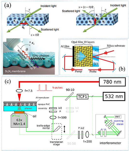
Figure 2. Experimental techniques used for probing hypersonic phonons. Schematic of (a) transmission and reflection scattering geometries in the BLS measurements. Reproduced from [100]. CC BY 4.0. And micro-BLS measurements on the surface wave. Reproduced from [101]. CC BY 4.0. And setups of (b) a pump-probe experiment. Reprinted (figure) with permission from [44], Copyright (2008) by the American Physical Society. (c) Hybrid pump-probe experiments. Reproduced from [106]. CC BY 4.0.
Download figure:
Standard image High-resolution image4.1. 1D hypersonic PnCs
The earliest studies of 1D PnCs pertain to semiconductor superlattices of which periodicity is few nanometers [122, 123]. From the Raman spectra [124, 125], the folded longitudinal phonon at THz was treated in the elastic continuum limit [122]. Expanding the periodicity to dozens of nanometers, Chen et al employed the picosecond ultrasonic technique to study the localized acoustic-phonon surface mode in the Al/Ag superlattices, the frequency of which depends on the periodicity [126]. However, a clear evidence of BG was reported later for hypersonic 1D PnCs. The first direct observation of a BG was realized in hybrid stacks with alternating silica (SiO2) and PMMA layers [60]. The dispersion relation, recorded by BLS, revealed the stopband occurred at the first Brillouin zone in the out-of-plane (periodicity) direction. The frequency and BG width are, however, reduced due to the porosity of the SiO2 layer. Triggered by this study, a full control of phononic band diagram through the oblique incident angle on the same system was achieved as shown in Figure 3(a) [59]. The frequency and width of BG along the periodicity direction varied with the oblique angle relatively to the axis normal to the sagittal plane of the film allowing thereby the estimation of the shear moduli of the individual layers. The inherent fabrication-related film imperfections, such as inhomogeneous layer thicknesses, blurred the position of the lower Bragg mode, but did not affect the width of the BG-type gap. However, if the layer-like defects breaks the symmetry of 1D PnC, the band structure becomes sensitive to the periodicity perturbations [120]. Schneider et al combined experiments with theoretical calculations to systematically investigate how the propagation of hypersonic phonons can be controlled by designed defects in the superlattices [120] as indicated in Figure 3(b). Introducing a defect layer at different positions in the superlattices (surface layer, inner cavity), the occurrence of both surface and cavity modes inside BG is clearly identified in the dispersion relation recorded by BLS. This study opened new pathways to the engineering of elastic waves in 1D PnCs. Besides defects, aperiodic structures of SL were revealed to exhibit better performance on tuning the bandgap than that of periodic structures [127]. Döring et al designed an aperiodic sample resembling a Fibonacci series along with the periodic structures of which reflectivity was measured by pump-probe technique [117]. Strong phonon mode confinement and phonon localization are expected, however, a lower resonance is found in the aperiodic system rendering such multiplayer structures attractive for new phononic applications [117].

Figure 3. Band structure of 1D PnCs (Poly(methylmethacrylate) (PMMA)/SiO2 superlattice). (a) Calculated dispersion relation is well overlapped with experimental data. The frequency of upper and lower branches of which defines the Bragg gap varies with incident angle. Reprinted with permission from [59]. Copyright (2012) American Chemical Society. (b) Introducing surface defect and cavity in the structure, the corresponding defect modes is observed in the band diagram. Reprinted (figure) with permission from [120], Copyright (2013) by the American Physical Society.
Download figure:
Standard image High-resolution imageDue to the small size, SAW PnCs show advantages for the integration in electronic integrated circuits over bulk wave-based PnCs. The SAW PnCs, with a grating pattern on the surface, possess new zone boundaries, zone folding, and band gaps [53, 128–132]. As the surface corrugations get much shallower than the SAW wavelength, SAWs propagating parallel to the grooves are not disturbed by the presence of the grating [128]. On the contrary, zone folding, bandgap, and local resonance interaction with bulk and surface waves occur when grooves depth is comparable to the SAW wavelength [57]. When defects are introduced into a periodic array of stripes coated on the surface, the localized branches, with frequencies governed by the defect size, appear in the bandgap induced by the anti-crossing of the Sezawa wave and zone-folded Rayleigh wave [130]. This outstanding structure-induced tunability of SAW enables 1D PnCs to be of great interest for practical applications [76]. Besides opening band gap, the Bragg reflector feature enables 1D hypersonic PnCs dominant applications in communication, specifically in making resonators, filters and oscillators using piezoelectric-based devices [133–136]. The acoustic Bragg reflectors, based on the constructive interferences, is first introduced by W. E. Newell who applied the optical Bragg reflectors in the acoustic fields in 1965 [137]. By miniaturizing the characteristic length to micro-scale, the acoustic resonator/filters are feasible for radio frequency (RF) applications. The implementation of 1D PnCs in the acoustic wave devices can suppress the acoustic leakage from devices, hence it is of an interest to many researchers and companies especially due to their potential applications in 5 G technology [138].
4.2. 2D hypersonic PnCs
The importance of controlling SAWs in modern technology is enormous. In their pioneering work, Tanaka and Tamura have theoretically predicted a stop band for SAWs in a 2D PnC consisting of square array of Al/As cylinders periodically embedded in a GaAs host matrix [139]. The modulation of SAW is subsequently realized in 2D PnCs devices [25, 28]. In analogy to 1D PnCs, the periodicity of inclusion leads to BG along certain symmetry direction. In addition to this effect, the inclusions can exhibit strong local and contact resonances leading to HGs [25]. As the modulation of elastic waves is structure and inclusion dependent, we deliberately present three different 2D PnCs, holey, pillar-based, and colloidal 2D PnCs with a monolayer of nanoparticles.
For holey 2D PnCs of a square lattice of holes on a SiO2/Si substrate [140, 141], the theoretically predicted dispersion with bandgap induced by Bragg reflection, quasi-Rayleigh and quasi-Sezawa surface waves [20] are experimentally confirmed by BLS [142] and pump-probe techniques [69, 116, 118]. Hou et al found the presence of nearly dispersionless shear-vertical-dominated branches in the high-wavevector range when the holes-Si interface is modified by a soft acrylic polymer layer as shown in Figure 4(a) [142]. This soft layer-induced acoustical isolation can facilitate the integration of the phononic film on a hard substrate.
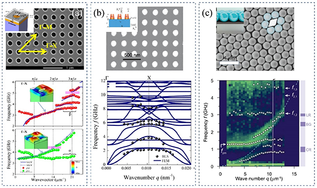
Figure 4. Experimental and calculated phononic band structures of 2D hypersonic PnCs. (a) Holey PnCs: antidot-patterned Permalloy sample with lattice constant a = 450 nm. Reprinted from [142], with the permission of AIP Publishing. (b) Pillar-based PnCs: Au pillars on 250 nm thick Si membrane. Reprinted (figure) with permission from [143], Copyright (2015) by the American Physical Society. (c) Colloidal PnC: Monolayer of PS nanoparticles on the Si membrane. BG, CR, and LR stand for Bragg, nanoparticle–membrane contact resonance, and local resonance gap, respectively. Reproduced from [101]. CC BY 4.0.
Download figure:
Standard image High-resolution imagePillar-based 2D PnCs [68, 69, 144–146], enhance the preceding possibilities for manipulating the elastic waves by opening additional HGs due to the strong interaction between the local resonances and the propagating waves [147, 148]. Yudistira et al fabricated cylindrical nanopillars arranged into a triangular lattice in lithium niobite, and observed the simultaneous existence of surface hypersonic band gaps from the band structure recorded by BLS [149]. The band gaps result from local resonances and Bragg scattering below the sound line (defined by the dispersion of bulk acoustic modes) at hypersonic frequencies [149]. This was the first demonstration of hypersonic bandgaps in 2D PnCs made of piezoelectric materials, enabling monolithic integration of photonics and phononics on the standard lithium niobite platform industry. Along this research direction, fabricated pillar-based PnCs on a complementary metal–oxide–semiconductor (CMOS) compatible piezoelectric platform allow direct integration of SAW-based devices with CMOS circuits on a single chip for multifrequency wireless applications [150]. Pillar-based PnCs possess, however, excessive elastic energy dissipation due to coupling between SAWs and bulk modes or pseudo-SAWs, limiting the performance of this structure. To overcome this deficiency, pillar-based PnCs membranes [96, 97, 144, 151], where the periodic arrays are decorated on a thin membrane with finite thickness, are proposed. In this configuration the achieved confinement of elastic waves tolerates exquisite performances of PnCs membrane-based devices-in waveguides [152] and filters. Figure 4(b) shows a pillar-based PnCs membrane composed of square lattices of holes/Au pillars on a Si membrane [64, 143]. For this structure, the dispersion relation recorded by micro-BLS (figure 4(b)) encompasses the effect of the Bragg scattering and the presence of the local resonances [143].
More recently, 2D colloidal PnC consisted of a monolayer of nanoparticles revealed a rich band structure. Employing the pump–probe technique [38, 114, 115, 153, 154], low-frequency contact-based modes of the granular monolayer, high-frequency modes originating from spheroidal vibrations of the microspheres and surface Rayleigh waves, were resolved [115]. The coupling between those modes led to the appearance of multiple band gaps in the 2D colloidal PnC membrane of figure 4(c) [101]. The frequency of bandgaps can be further tuned by the particle size and interactions between particle-particle and particle-substrate [37]. Considering the low-cost mass production of the self-assembly process, the colloid-based PnCs present a robust platform for fundamental studies and have potentials of signal processing for wireless communications.
4.3. 3D hypersonic PnCs
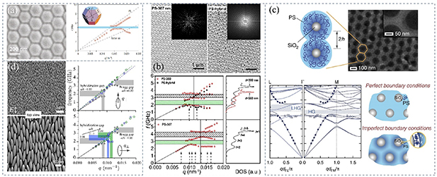
Despite the complexity of 3D structures, several groups employed the facile self-assembly method to construct 3D building blocks, typically consisting of the particles homogeneously dispersed in the liquid or solid matrix [27, 36, 42, 45, 155]. There are few experimental studies (figure 5) on 3D hypersonic PnCs compared to the photonic analogues and the understanding of the phononic band diagram is, in spite of the theoretical efforts, still incomplete [110, 111, 156]. The first direct experimental evidence of BG at hypersound range in 3D PnCs was reported by Cheng et al [45] shown in figure 5(a). The structure of PnCs consisted of the face-centered-cubic colloidal crystals formed by self-assembly of PS nanoparticles with subsequent fluid infiltration. The BG opens for finite elastic impedance between nanoparticles and fluid host. Boosting the elastic mismatch by infiltration polydimethylsiloxane (PDMS) in the same opals leads to the simultaneously observation of a HG [99] in figure 5(b). This HG is expectedly robust to the disorder in contrast to the structural-sensitive BG and opens near but below the particle fundamental resonance mode. The assignment of this HG to the anti-crossing effect between the quadrupole (l= 2) particle mode and effective medium propagating acoustic wave is theoretically true for solid/liquid topology [110] realized for colloidal suspensions below the close packing [111]. Inspired by these pioneering work, for solid/solid colloidal crystals realized by crosslinked PDMS host, the observed single gap is assigned to a BG-type [109]. The consolidation of the PS particles might imply an inverse (liquid/solid) topology that should display HG but not associated with the particle quadrupole mode. More recently, Alonso-Redondo et al proposed a new strategy to realize HG in self-assembled polymer-tethered silica colloidal films [100] by harnessing the 'anisotropic elasticity' across the particle–polymer interface [157] shown in figure 5(c). In this real solid/solid topology, a flat band from the degenerate fundamental torsional mode (l = 1) of the single silica sphere was for the first time observed at submicrometric scale [100]. Replacing the spherical nanoparticle with anisotropic ellipsoids in a liquid host, the HG was observed to be direction-dependent in figure 5(d), suggesting acoustic anisotropy that was observed for only macroscale acoustic metamaterials till then [93].
Figure 5. Characterization on the phononic band diagram of 3D PnCs. (a) Wet opal consisting of polystyrene (PS) nanoparticles infiltrated with silicon oil; the dash lines in dispersion relation denoted the acoustic branch of pure PS and silicon oil. Reprinted by permission from Springer Nature Customer Service Centre GmbH: [Springer)] [Nature Materials] [45] (2006). (b) PS and PS-hybrid crystals infiltrated with liquid PDMS; the density of states spectra of single PS particle in PDMS is shown in the right-hand of phononic band diagrams of wet PS crystals. The hatched areas marked the BG and HG gaps. Reprinted (figure) with permission from [99], Copyright (2008) by the American Physical Society. (c) Particle brush consisting of PS-tethered silica particles; the theoretical band diagram along with experimental data of a particle bursh film; schematic presentations of perfect and imperfect boundary condition models applied at the PS-silica interface. Reproduced from [100]. CC BY 4.0. (d) Aligned ellipsoids infiltrated with PDMS; anisotropic dispersion relations along the orthogonal directions. Reprinted (figure) with permission from [93], Copyright (2014) by the American Physical Society.
Download figure:
Standard image High-resolution image
5. Perspectives
Hypersonic PnCs, with periodicity in sub-micrometer range, demonstrate excellent capability to manipulate the propagation of elastic waves at gigahertz frequencies by means of Bragg scattering, local resonances, and defects. The high operation frequency offers hypersonic PnCs potential applications, especially in the fields of information and communication technologies. Therefore, tailoring the band structures of new structures and materials at hypersonic regime along with the fabrication technology in sub-microstructures will continuously receive strong research interest.
Engineering of the PnCs with periodicity in hundreds of nanometers can be achieved by microfabrication [52], such as microlithography [158] and etching [159], and self-assembly. These technologies are mature in terms of their capability to tailor the microstructure with high precision. The self-assembly approach is best-suited for the colloidal PnCs of which structures can be homogenous or heterogeneous [36]. In contrast, microlithography can access versatile and complex architectures from 0D to 3D, and it is the commonly used and powerful tool for nanofabrication in spite of disadvantages such as complexity and time consuming [55]. The central frequencies of bandgaps in those PnCs are about dozens of gigahertz, while, to achieve a higher frequency in the order of hundreds of gigahertz, nanosized inclusions are required. The low-dimensional nanomaterials, e.g. nanotubes [160] and quantum dots [161, 162], are good choices as building blocks, however, their ultra-small dimensions yield their phononic characterizations difficult [1]. A hybrid approach [121] based on combining a pulsed laser for phonon generation (as in pump-probe spectroscopy) with a tandem Fabry–Perot interferometer (as in BLS) was proposed for characterizing the bandgap of non-transparent 1D PnCs that cannot be accessed by BLS, a unique tool for determining the dispersion relation [106]. Although there are still no decisive advantages of the hybrid technique over conventional pump-probe spectroscopy, this study provided the feasibility for overcoming the limitations that time- and frequency-domain approaches exhibit separately. Nevertheless, further developments on the characterization instruments are critical for the experimental investigation on the PnCs comprised of nanomaterials.
The comparable structural length scales, i.e. sub-micrometer ranges, of hypersonic PnCs and PhCs in the visible spectrum allow simultaneously manipulating the elastic and electromagnetic waves [163, 164] by tailoring material properties, such as the dielectric constant, mass density, elastic constants, and geometric parameters, such as periodic patterns and scatter shape. This unique structure, termed as phoxonic crystals (PxCs) [164], presents band gaps for hypersound and visible light concurrently, evoking a thrilled perspective for modulation on the light–matter interaction [165]. Optomechanical coupling is one of the most important features of photon–phonon interaction, which refers to the co-localization of GHz phonons and telecom photons that can modify the propagation of hypersonic phonons simultaneously with that of the photons (at similar wavelengths but much higher frequencies [166]). A proper designed defect in the PnCs could amplify the optomechanical coupling, shading light on the integration of multifunctional optomechanical circuits on a single chip [31, 167, 168]. Given the ability of phonon to strongly interact with microwave [103] in addition to telecom photons [169], the cavity optomechanics was applied to the microwave-to-optical transductions, which turn out to be a landmark application for electro-optomechanical systems [105, 170–173]. Mechanically mediated microwave-to-telecom transducers based on the high-frequency mechanical motion has received a great deal of interest, opening the prospect for a new application-orientated field for hypersonic PnCs [112, 171, 174, 175].
Acknowledgments
Y C acknowledges the financial support by Shanghai Pujiang Program (Grant No. 20PJ1413800) and National Natural Science Foundation of China (Grant No. 12102304). G F acknowledges the financial support by ERC AdG SmartPhon (Grant No. 694977).
Data availability statement
No new data were created or analysed in this study.