

Abstract
Photonic structures have been attracting great attention as they have the ability to manipulate the photoresponse. Here, we report a hole array for effective photon trapping, therefore facilitating optoelectrical conversion of a midwave infrared photodetector. The integrated device consists of an InAsSb-based heterojunction photodiode and an embedded symmetric hole array penetrating through the top wide bandgap layers into the absorption region, which enables lower dark current, better broadband absorption, and improved polarization-independent photoresponse. The photoresponse enhancements of 26%–170% are achieved in the 2–5 µm range under zero power supply at temperatures from 293 K to 78 K. Combined with the effect of slightly decreasing in bulk dark current density, the zero-bias detectivity is increased by 29% at room temperature without sacrificing the response speed, where the enhanced detectivity increases to 2.09 × 10⁹ Jones. This proposed approach provides a new strategy to boost optoelectrical conversion of photodetectors, thereby facilitating robust photodetection for widespread applications.
Export citation and abstract BibTeX RIS
1. Introduction
Incorporation of photonic structures is widely regarded as an effective way to realize high-performance photodetection as the raised light–matter interaction inside detection layer can facilitate light absorption without sacrificing the response speed [1–4]. Integrating the plasmonic structure is one of the most popular strategies, since at the metal–dielectric interface, the optical field can be enhanced by the surface plasmon resonance [5–9], thus resulting in the increase of absorption. Another approach to improve the photoresponse is to utilize Fabry–Pérot or other resonant structure surrounding absorption layer [10]. While it does enhance quantum efficiency, the wavelength selectivity of cavity resonance behavior requires the perfect match between the cavity resonance wavelength and bandgap of device absorption layer.
An embedded photon-trapping (PT) structure is considered to be a good choice for better light manipulation. With the help of PT structure, the combined effects of the resulted lateral propagating modes and reduced effective refractive index can bring various advantages, such as polarization-independent broadband absorption enhancement and reduced bulk dark current. Recently, PT structure has been proved useful to improve optical performance in visible wavelengths for solar cell, optical communication links [11, 12], as well in near infrared regime for single-photon avalanche detectors [13].
The atmosphere midwave infrared (MIR) range (2–5 µm) is of great significance for security, medical diagnosis and military applications [14, 15]. The drive towards high-sensitivity, high-operating-temperature and robust MIR photodetection has stimulated considerable research efforts, which mainly lies in adopting external plasmonic or other resonant structures. In this work, we design an InAsSb-based hetero-n–i–p photodiode with an etched PT hole-array structure to improve absorption efficiency, thus obtaining a MIR photodetector with enhanced detection performance. Using a set of simulated optimal geometric parameters to fabricate, a 38% absorption enhancement is obtained at 3 µm. As such, a broadband photoresponse improvement of 26% is achieved in the wavelength range of 2–5 μm. Besides, dark current density is also reduced due to decreased bulk volume by the etched PT structure. In this way, a zero-bias room-temperature detectivity enhancement of 29% higher than the reference detector without PT structure is obtained, where the enhanced detectivity increases to 2.09 × 10⁹ Jones. When the temperature drops to thermoelectric cooling (TEC) temperatures of 260 K and 243 K, the detectivity enhancement can even reach to more than two- and three-times. A response speed as fast as that of the reference is also observed. To this end, the etched PT structure does realize the polarization-independently broadband photodetection improvement for robust applications.
2. Materials and methods
2.1. Device design
The schematic diagram of the hetero n–i–p photodetector integrated with PT hole array is shown in figure 1(a), where the cylindrical hole array is in hexagonal lattice. The targeted device comprises a InAsSb-based heterojunction n–i–p architecture grown on GaSb substrate, where the absorption i-layer is composed of InAs0.912Sb0.088 with a thickness of 1.5 μm. In a conventional homojunction photodiode, large dark current is always the major obstacle for obtaining good performance. To improve on that, the basic device not only adopts the heterojunction architecture, but also includes a highly doped wide-bandgap p-AlGaSb layer between the GaSb contact layer and InAsSb absorption i-layer to prevent the minority carrier (electron) diffusion. Such high doping also facilitates high electron concentration without inducing obvious bandgap narrowing. The lattice-matched layers with different bandgaps are grown by RIBER-32 molecular beam epitaxy system, where the specific layer parameters are indicated in table 1. High resolution x-ray diffraction and photoluminescence spectra indicate high-quality interfaces and absorption layer [16]. In this way, the basic heterojunction photodetector obtains relatively low dark current and high sensitivity for MIR detection.
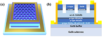
Figure 1. Hetero n–i–p photodetector with PT hole-array structure. (a) Schematic diagram of the hetero photodiode with the PT structure (cylindrical hole array in hexagonal lattice) etched to the absorption layer. (b) Cross-section diagram of hetero photodiode with micro-structured holes.
Download figure:
Standard image High-resolution imageTable 1. Layer parameters of the hetero-n–i–p photodetector.
| Material | Composition | Thickness | Doping |
|---|---|---|---|
| GaSb | — | 50 nm | ND ∼ 2 × 1018 cm−3 |
| Alx In1−x Asy Sb1−y | x = 0.15; y = 0.009 | 20 nm | ND ∼ 2 × 1018 cm−3 |
| InAsy Sb1−y | y = 0.912 | 1500 nm | Intrinsic |
| Alx In1−x Asy Sb1−y | x = 0.2; y = 0.912 | 20 nm | NA ∼ 2 × 1018 cm−3 |
| Alx Ga1−x Sb | x = 0.42 | 40 nm | NA ∼ 2 × 1018 cm−3 |
| Alx Ga1−x Sb | x from 0.42 to 0.1 | 30 nm | NA ∼ 2 × 1018 cm−3 |
| Buffer GaSb (Be) | — | 1000 nm | NA ∼ 2 × 1018 cm−3 |
| Substrate GaSb (Te) | — | 600 μm | ND ∼ 7 × 1017 cm−3 |
We then manage to integrate the hetero photodetector with the PT hole-array structure, where microscale holes are etched through the top contact layer to reach the absorber, for promoting absorption efficiency and thus increasing the photoresponse capability. The corresponding cross-sectional diagram is shown in figure 1(b). To quantify the performance enhancement of the PT structure, we regard the detector without PT structure as the reference (ref) detector and the device integrated with the PT structure as 'PT detector', both with the same absorption area.
2.2. Simulations
Finite-difference time-domain method is used to analyze the light confinement capability and wave propagation condition in PT detector. It is turned to calculate the absorption of patterned photodetector through transmittance and reflectance, as well as the electric field distribution in the structure. The detailed simulation setting is described in appendix
Figure 2(a) illustrates the simulated absorption spectra of the PT detector in its optimal geometrical parameters, and the ref detector. It is observed that the absorption is obviously enhanced by integrating the PT structure, where the maximum enhancement rate of 55% is obtained at wavelength of 3 μm. The integrated absorption value, as an index to quantify the optical performance enhancement, is defined as the ratio of absorbed optical power to incident power over the wavelength range of 2–5 μm [17]. The simulation results indicate a maximal integrated absorption value of 56% for the PT detector. Compared with the 40% for the ref detector, a significant 38% absorption improvement is achieved. Meanwhile, the absorption value is quite robust with the change of geometrical parameters as a 5% variation in geometrical parameters only results in about 1% change in the integrated absorption. This characteristic is helpful in facilitating large-scale production. As a confirmation, we also performed simulation on the absorption by integrating per unit volume, as indicated in figure 9. The results obtained from integration (Pabs_tota) are almost the same as those derived from transmission and reflection.
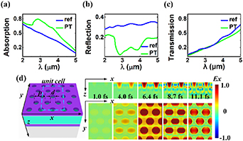
Figure 2. Simulation results for the ref and PT detectors. Simulated (a) absorption spectra, (b) reflection spectra and (c) transmission spectra in 2–5 μm range. (d) The electric field distribution change with light propagation in PT detector at λ = 3 μm, that is, the Ex component of the field with time increasing from left to right. Top row: x–z plane. Bottom row: x–y plane. Light illuminates the holes in the z direction. Time from left to right: t = 1.0, 4.0, 6.4, 8.7, 11.1 fs. The field first goes into the hole and then spreads laterally into the photodetector as cylindrical waves. The top view of the unit cell for simulation is also shown on the right of (c), where 'p' represents the period between the holes, and 'd' represents the hole diameter.
Download figure:
Standard image High-resolution imageTo explore the light trapping mechanism in the PT structure, the simulated reflection spectra are presented in figure 2(b). It is observed that the reflection of PT detector is obviously lower than that of the ref detector, while the simulated transmission spectra are almost same (figure 2(c)). In this way, the reduction of reflection can almost directly reflect the absorption increase in the PT detector. The integrated reflection value between 2 and 5 μm for the PT detector is only 15%, much smaller than the 34% of ref detector. Thus, one of the roles of the PT-structure is to reduce reflection due to the reduced volume filling factor (ff = volume of air/volume of material) which is described as:
The corresponding effective refractive index (neff) of the PT hole array is thus reduced which is expressed in the following formula [18]:
where  i and b are the dielectric constants of air and background material (hetero InAsSb-based n–i–p, ∼15 [19]), respectively. As a result, the reduced refractive indices will lead to a reduced reflection, as derived from the equation (3):
By taking the optimal parameters (p = 3 µm, d = 0.67p) into the mathematic model, the calculated R is 21% with a neff of 2.67, which is consistent with the value of wavelengths below 2.5 µm and above 4.5 µm for PT detector. While the calculated R of the ref detector is 34% with a neff of √b equal to 3.88, which corresponds to that of wavelengths from 2 to 5 µm for ref detector. Also, it is remarkable to note the effect of reflection reduction is more significant at wavelengths between 3 and 4 µm, where the reflection value is around 10%.
Figure 2(d) shows the Ex
component of electric field distribution changing with time in the PT detector under a normal plane wave illumination. To better observe the light propagation, the unit cell in simulation contains eight holes, whose area is expressed as: 2p × 2p × tan60°, since the separate distance between two neighboring holes in y-direction of the hexagonal lattice is ptan60°. The transient evolution of Ex
distribution from t = 1.0 to 11.1 fs is depicted in the figure. The results show that the waves in lateral direction gradually appear around holes and form the collective lateral propagating modes. In order to clearly present the bending of light propagation direction, Poynting vector distribution is shown in appendix
Besides, it is reported when the period of PT hole array is set close to the wavelength of the absorbed light, the group velocity of the modes can be treated as slow modes in photonic crystal, leading to more chances for stimulating laterally propagating modes [22, 23]. It thus explains why we can achieve an obviously enhanced absorption at wavelengths around 3 µm with the period of PT structure set to 3 µm [16]. In this way, the incident light propagating in PT hole arrays can obtain a large k|| which makes light interaction in absorption layer more efficient [24].
Therefore, in the case of hetero-n–i–p detector assisted by the PT structure, the absorption enhancement can be attributed to the combination effects of lateral propagating modes around the resonant wavelengths and reduced reflection due to lower effective refractive index of the PT structure. In addition, the etched hole array also reduces the physical volume of the device. It can help to limit the bulk dark current, which is the main obstacle for MIR detector operating at room temperature [25]. As such, the decreased bulk dark current can balance or even overwhelm the increased surface leakage by extra exposed areas induced from the etched PT structure.
3. Results and discussion
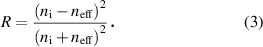
The PT hole array in its simulated optimal geometrical parameters was fabricated on the InAsSb-based heterojunction n–i–p photodiode. The corresponding SEM profile is shown in figure 3(a). The absorption spectra are then obtained by measuring the transmission and reflection via Fourier transform infrared (FTIR) spectroscopy, as shown in figure 3(b). Compared to ref detector, it is demonstrated that a 38% absorption enhancement is obtained at 3 µm in PT detector. Due to the continually distributed incident angles which are up to about 30° mainly from the condenser in the FTIR experimental set-up (36× objective lens (NA = 0.5)), the measured reflection spectra demonstrate broadband feature with a wider peak, compared with the simulation results under normal incident light [26]. Meanwhile, the absorption of ref and PT detectors at different polarization angles were measured (figure 3(c)) and the results show the polarization-independent property of the PT structure, which is in consistent with the simulation result shown in appendix
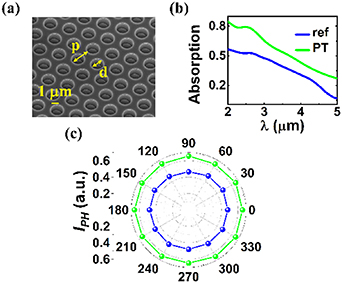
Figure 3. Fabricated PT hole arrays and measured absorption spectra. (a) The SEM profile views of the PT hole array, parameterized by period p and hole diameter d, where the scale bar is 1 μm. (b) Measured absorption spectra of the ref and PT detectors in the wavelength range of 2–5 μm. (c) Measured absorption at 3 μm of the ref and PT detectors for different polarization angles.
Download figure:
Standard image High-resolution imageFor device fabrication, the corresponding schematic diagrams of detailed fabrication process and SEM image of the fabricated device are shown in appendix
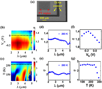
Figure 4. Photoresponse enhancement of PT detector relative to ref detector. (a) SEM image of the fabricated PT detector. (b) At room temperature (293 K), enhancement factor (η) of photocurrent (IPH) spectra in the range of 2–5 μm measured under the bias from −0.3 V to 0.1 V at room temperature (293 K). (c) η of IPH spectra at temperatures from 78 K to 293 K under zero bias. (d) Extracted room-temperature η of IPH spectrum under 0 V. (e) Extracted η of IPH spectrum under 0 V at 260 K. (f) The average value of the η integral from 2 to 5 μm at room temperature under the bias from −0.3 V to 0.1 V. (g) The average value of the η integral from 2 to 5 μm under zero bias at different temperatures.
Download figure:
Standard image High-resolution imageWe used a 1000 K blackbody radiation source to measure the detector responsivity in the mid-infrared range. The responsivity is defined as RA = Is/Pinc, where Pinc is the incident power radiated on detector and Is is the signal current generated by fabricated detectors. Appendix
Figure 5. Comparison of responsivity, noise and detectivity of the ref and PT detector. Responsivity (RA) versus (a) bias and (b) temperature, noise (vn) versus (c) bias and (d) temperature. (e) Dark current density characteristics. Detectivity (D*) versus (f) bias and (g) temperature.
Download figure:
Standard image High-resolution imageFor the noise (vn) characteristic shown in appendix
Finally, the response waveform in reaction to a 2.94 μm laser source is shown in figure 6(a), where the corresponding rise and fall time are around 1.4 μs and 1.2 μs for ref and PT detectors, respectively. It is relatively lower than the current high-speed detection, which may be originated from the different detection mechanism and RC time delay [38]. Figure 6(b) shows the amplitude–frequency response (f−3dB) values which are 2.4 × 10⁵ Hz and 3 × 10⁵ Hz for the ref and PT devices, respectively. The slightly better frequency response is mainly due to the faster collection of the photogenerated carriers as the physical holes shorten the transportation path for the carriers generated after absorbing the photons reaching the bottom of the holes.
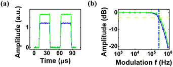
Figure 6. Frequency response of the ref and PT detector. (a) Response waveform under zero bias. (b) Amplitude–frequency response.
Download figure:
Standard image High-resolution image4. Conclusion
This article presents the design and fabrication of PT detector which is an InAsSb-based hetero-n–i–p MIR photodetector with etched hole array structure. With assistance of this polarization-independent PT structure, the resulted lateral propagating modes and reduced effective refractive index can enhance light absorption, leading to a broadband absorption improvement of 43% in the wavelength range from 2 to 5 μm. The PT hole array also reduces bulk dark current. A room-temperature detectivity of 2.09 × 10⁹ Jones is obtained under zero bias, which is 29% higher than that of reference detector without photonic cavity structure. In addition, at TEC temperatures of 260 K and 243 K, the detectivities are about 5.75 × 10⁹ Jones and 7.97 × 10⁹ Jones without applied bias, which correspond to two- and three-times enhancement compared to that of the reference detector. The work provides an effective alternative for enhancing mid-infrared photodetection.
Acknowledgments
This work was supported by A*Star (SERC A1883c0002 and 1720700038), Singapore. Fei Suo and Jinchao Tong contributed equally to this work.
Data availability statement
The data that support the findings of this study are available upon reasonable request from the authors.
Appendix A.: Numerical simulation of PT hole array structure
A.1. Simulation setting
The absorption spectra and electric field distributions of the detector integrated with a PT structure were calculated using a commercial finite difference time domain software (FDTD Solutions, Lumerical Inc.). The periodic boundary conditions were used in the lateral direction of unit cell to simulate an infinite periodic array of the PT structure on detector and the perfectly matched layer conditions were employed in the longitudinal z-direction. The mesh size was set to 5 nm in all simulations. The dielectric constant of the hetero-n–i–p photodiode was obtained from previously reported data [39]. The detector was illuminated with the plane waves and the absorption spectra were calculated by subtracting transmission and reflection, where the power monitors for reflection and transmission are positioned above the detector structure and below the substrate, respectively.
A.2. Parameter optimization for PT hole array structure
To optimize parameters of PT structures for realizing maximum MIR light absorption, we use Lumerical FDTD solution to simulate light absorption in the designed hetero n–i–p photodetector with the PT cylindrical hole array in hexagonal lattice (CH).
Firstly, the absorption of hetero-n–i–p photodiode with the PT structure at λ= 3 μm is simulated by simultaneously scanning hole array period (p) and ratio of hole diameter to period (rd), defined by d/p, where the hole depth is initially set at 1 μm. The scanning range of p is set around the peak wavelength response of our InAsSb-based photodiode, and the rd range is chosen in between 0.4 and 0.7 as we consider the practicability of the detector. The corresponding simulation results are shown in figure 7(a). Furthermore, figure 7(b) shows the range of hole depth (D) scanned from 0.5 μm to 1.3 μm at per step of 0.1 μm in the wavelength (λ) ranging from 2 μm to 5 μm under the previously simulated optimal p and rd.
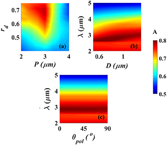
Figure 7. Simulated absorption (A) results of PT structure (cylindrical hole array in hexagonal lattice (CH)) on the hetero-n–i–p photodiode. (a) Simulated absorption at λ = 3 μm by simultaneously scanning period (p) and ratio of hole diameter to period (rd). (b) Simulated absorption by simultaneously scanning hole depth (D) and λ. (c) Simulated absorption at polarization angles from 0 to 90°.
Download figure:
Standard image High-resolution image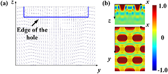
Figure 8. Simulated lateral propagating modes in the detector with PT structure. (a) Poynting vector direction. (b) The corresponding Ex component of the field (top row: x–z plane, bottom row: x–y plane).
Download figure:
Standard image High-resolution image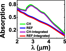
Figure 9. Simulated absorption spectra for the ref and PT detectors by using the way of derivation from reflection and transmission, and integrating the absorption per unit volume.
Download figure:
Standard image High-resolution imageThose calculations are performed by selecting a set of optimal topological parameters of PT hole array structure for obtaining a maximized absorption in the photodetector, which can then be used as the guideline for the PT hole array fabrication. The corresponding optimal parameters derived from the simulation results are p= 3 μm, rd from 0.67 to 0.72, and D⩾ 1 μm. Considering fabrication and effective absorption of light, we select 1 μm as the hole depth. Likewise, the optimal rd is chosen with the smallest value among the selected range.
In addition, to verify the polarization independence of the PT structure, the absorption simulation is implemented by simultaneously scanning polarization angle (θpol) and λ, with optimized p, rd and h values. As shown in figure 7(c), the PT structure possess the feature of polarization independence of the incident light due to the structure symmetry, which is good for practical applications.
A.3. Poynting vector distribution
A.4. Simulated absorption per unit volume
Appendix B.: Device fabrication
The detailed fabrication process schematic diagrams are described in figure 10. In order to check the effectiveness of PT structure, the hetero-n–i–p photodiode without the PT hole array is also fabricated as the reference device. The fabrication of reference device starts from the step of lithography for mesa pattern define, followed by the same steps as PT devices.

Figure 10. Schematic diagrams of fabrication process flow for hetero-n–i–p photodiode integrated with PT hole array structure.
Download figure:
Standard image High-resolution image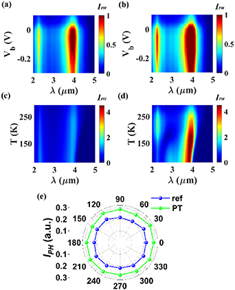
Figure 11. Comparison of photocurrent spectra for ref and PT detector. At room temperature (293 K), the photocurrent (IPH) spectra under the bias from −0.3 V to 0.1 V for (a) ref and (b) PT detectors. Under the bias of 0 V, the IPH spectra at temperatures from 78 K to 293 K for (c) ref and (d) PT detectors. (e) IPH at 3 μm of two detectors for different polarization angles at room temperature under zero bias.
Download figure:
Standard image High-resolution image
Figure 12. Comparison of responsivity, noise and detectivity for ref and PT detectors. The responsivity (RA) under the bias from −0.3 V to 0.1 V and at temperatures from 78 K to 293 K for (a) ref and (b) PT detectors. The noise (vn) under the bias from negative to positive at temperatures from 78 K to 293 K for (c) ref and (d) PT detectors. The detectivity (D*) under the bias from −0.3 V to 0.1 V and at temperatures from 78 K to 293 K for (e) ref and (f) PT detectors.
Download figure:
Standard image High-resolution image
B.1. PT hole array pattern define and surface passivation
A 150 nm thick SiO2 layer was deposited by chemical vapor deposition (CVD) on the top of this InAsSb-based hetero-n–i–p material to serve as a hard mask during the etching of PT hole array structure, which would be later removed by buffered oxide etch (BOE). The material was then patterned by electron-beam lithography, in which the 250 nm thick ZEP520A positive-tone photoresist was exposed under 20 keV electron gun voltage and 35 pA beam current. After that, development in n-amyl acetate (ZED-N50) for 20 s and rinse in methyl isobutyl ketone for 20 s were done at room temperature. The process parameters have been tuned in order to realize the designed optimal topological parameters of the PT pattern (hole array period p, ratio of hole diameter to period rd). Following that, reactive-ion etching (RIE) was used to transfer the PT pattern on SiO2 hard mask, with a 240 s process of 30 sccm CF4 and 30 sccm CHF3 flow at 15 mTorr and 170 W power. Then the patterned photoresist was removed by acetone and oxygen plasma. The device material was finally etched through the SiO2 mask by the high-temperature inductively coupled plasma-reactive ion etching (ICP-RIE) at 250 °C, using 8 sccm Ar, 2 sccm Cl2 and 4 sccm BCl3, at a direct current bias of 125 V, with an ICP power of 400 W and a RF power of 140 W for 80 s. After etching, the exposed PT hole array surface was passivated by piranha solution, a mixture of sulfuric acid (H2SO4), deionized (DI) water, and hydrogen peroxide (H2O2). The SiO2 hard mask was then removed by BOE. As shown in the SEM profile in figure 3(a), the vertical sidewalls of PT pattern, and the reasonable uniformity of the fabrication deviation error within 5% are obtained in device material. In this way, the topology parameters of each PT structure are corresponding to their respective optimal simulation results.
B.2. Mesa etch and surface passivation
The define of mesa pattern on device material was implemented by generic lithography process, using MJB4 mask aligner with the exposure wavelength of 365 nm and AZ5214 positive tone photoresist, spun after a hexamethyldisilazane (HMDS) adhesion promoter coating. Then the sample was developed in the diluted AZ developer (developer:water = 1:2) for 2 min and then rinsed in DI water. Following the mesa patterned on photoresist by development, the sample was etched through by wet etching method, with the etching solution mixed with phosphoric acid (H3PO4), citric acid, hydrogen peroxide (H2O2) and DI water. As a result, the mesa depth of 1800 nm was obtained after photoresist removal. A 300 nm thick SiO2 passivated layer was then deposited on top of the sample by CVD.
B.3. Window open for light absorption and electrodes
The windows opening for light absorption and electrodes in the passivated SiO2 layer was through standard lithography with the exposure wavelength of 365 nm and AZ2035 negative tone photoresist, spun after a HMDS adhesion promoter coating. The use of AZ2035 resist is well-suited for fully covering the top and bottom depth difference of mesa, as its thickness can be achieved up to around 3.5 µm through controlling spin coating speed, and its resolution also fits for the critical dimension requirement of window opening. After pattern transferring to the photoresist, RIE was used to etch passivated SiO2 layer for opening window, with a 480 s process of 30 sccm CF4 and 30 sccm CHF3 flow, at 15 mTorr and 170 W forward power. The patterned photoresist was then removed by acetone and oxygen plasma.
B.4. Electrode deposition
Finally, the same standard lithography as above window opening steps was adopted for the define of top and bottom electrode pattern. The electrical contacts of 20 nm thick titanium (adhesion layer) and 280 nm thick gold on top and bottom GaSb layer were then formed by electron beam evaporator system and standard lift-off process.
Appendix C.: Performance characterization
The Fourier transform infrared (FTIR) spectrometer equipped with a microscope (Vertex 70, Bruker) was used to characterize the reflection and transmission spectra of photodiodes w/o PT structures. In the measurement setup, a MIR source, an infrared polarizer, a KBr beam splitter, a mercury–cadmium–telluride (MCT) detector and the HYPERION Series FTIR Microscopy and Imaging System with a 36× objective (NA = 0.41) were used to collect the optical signal in 2–5 μm range. Then the collected light signal was normalized with the background spectra of gold pad (for reflection) and GaSb substrate (for transmission). To facilitate the photodetection performance characterization, the fabricated devices were mounted and wire-bonded to the ceramic chip carrier. The current–voltage (I–V) characteristics were performed by the SC-200 mm probe station with the B1500A semiconductor parameter analyzer. The MIR responsivities were obtained from the blackbody light source (at 1000 K) passing through the optical bandpass filter (2.5–4.8 μm) and mechanical chopper, where the blackbody photocurrent signal generated by photodetector was read out by a Lock-in amplifier (EG&G 7260 DSP) after being converted into a photovoltage by a low noise current pre-amplifier (model SR570, Stanford Research Systems). The photocurrent spectra in MIR range were also measured by the FTIR using a MIR source and focusing lens, but with our fabricated detectors w/o PT structures instead of its internal MCT detector to convert optical signal into electrical signal. The response waveform was measured using a 2.94 μm laser with pulse repetition frequency varied from 1 kHz to 1 MHz. The pulse width of the reference signal was thus varied with the repetition frequency while the rise and fall times are both fixed at ∼20 ns. The output power of the laser source for different modulation frequencies was calibrated by a standard power meter. For the measurement performed at different temperatures (78–293 K), the samples were mounted in a cryogenic thermostat in front of the ZnSe window (Optistat DN-V, Oxford Instruments), with the high-vacuum condition (below 10−5 mTorr).