
Abstract
The tunable electronic structure of graphene nanoribbons (GNRs) has attracted much attention due to the great potential in nanoscale electronic applications. Most methods to produce GNRs rely on the lithographic process, which suffers from the process-induced disorder in the graphene and scalability issues. Here, we demonstrate a novel approach to directly grow free-standing GNRs on step-bunched facets of off-oriented 4H-SiC epilayers without any patterning or lithography. First, the 4H-SiC epilayers with well-defined bunched steps were intentionally grown on 4 degree off-axis 4H-SiC substrates by the sublimation epitaxy technique. As a result, periodic step facets in-between SiC terraces were obtained. Then, graphene layers were grown on such step-structured 4H-SiC epilayers by thermal decomposition of SiC. Scanning tunneling microscopy (STM) studies reveal that the inclined step facets are about 13–15 nm high and 30–35 nm wide, which gives an incline angle of 23–25 degrees. LEEM and LEED results showed that the terraces are mainly covered by monolayer graphene and the buffer layer underneath it. STM images and the analysis of their Fourier transform patterns suggest that on the facets, in-between terraces, graphene is strongly buckled and appears to be largely decoupled from the surface.
Export citation and abstract BibTeX RIS

Original content from this work may be used under the terms of the Creative Commons Attribution 3.0 licence. Any further distribution of this work must maintain attribution to the author(s) and the title of the work, journal citation and DOI.
Introduction
Recently, graphene nanoribbons (GNRs) have attracted much research interest for future nanoelectronics due to their unique electronic properties, such as ballistic transport or the bandgap scaling with the width of GNRs [1–5]. Several methods for the fabrication of the GNRs have been demonstrated, including unzipping carbon nanotubes, surface-assisted assembly of molecular precursors, chemical exfoliation, as well as sublimation on a lithographically structured SiC substrate [4, 6–12].
So far, most methods to produce GNRs rely on the lithographic process, which can result in disordered and rough edges. These defects significantly deteriorate the electronic properties of GNR [13, 14]. Recently, many works reported a promising way for growth of GNRs by a selective sublimation growth of graphene on the sidewalls of SiC (0 0 0 1) mesa structures [3, 5, 9, 15], which were still relying on the lithographic process. In this work, we demonstrate a novel approach to directly grow free-standing GNRs on step-bunched facets of off-oriented 4H-SiC epilayers without any patterning or lithography.
SiC homoepitaxial layers grown on the off-axis SiC (0 0 0 1) substrates usually exhibit a pronounced step bunching phenomenon, which has been interpreted as a result of minimizing surface free energy. Such SiC homoepitaxial layers with well-defined bunched steps are superior for the formation of GNRs on step facets, given the fact that the nucleation of graphene starts from step facets preferentially where the highest density of dangling bonds exists [16]. For instance, it was reported that the bilayer graphene was formed on the step facets while the monolayer graphene was grown on (0 0 0 1) terraces on off-oriented 4H-SiC substrates [4, 17]. Interestingly, it is already known that the buffer layer delaminates on the step facets instead forming free-standing graphene [18].
In this work, we first grew 4H-SiC homoepitaxial layers on commercial 4° off-oriented 4H-SiC(0 0 0 1) substrates by sublimation epitaxy. Due to the pronounced step-bunching during growth, the 4H-SiC epitaxial layers exhibit periodic step facets in-between terraces, which are purposely used for the growth of free-standing GNRs. The surface morphology was characterized by atomic force microscopy (AFM), and the number of graphene layers were determined via micro-Raman spectroscopy, low energy electron microcopy (LEEM), and micro-low energy electron diffraction (µ-LEED). The graphene formed on the step facets was further studied by atomically resolved scanning tunneling microscopy (STM).
Experimental details
The 4H-SiC homoepitaxial layers were grown on commercial 4° off-oriented 4H-SiC(0 0 0 1) substrates at 1850 °C by a sublimation epitaxy technique. The growth setup has been well described in a previous work [19]. Briefly, the 4H-SiC(0 0 0 1) substrate and a polycrystalline SiC source material was separated by a graphite spacer in an inductively heated graphite crucible. The substrate was heated up to 1850 °C with a ramping rate of 30 °C min−1, and the temperature was kept for 10 min. After the growth of 4H-SiC epilayers, the samples were cooled down to room temperature. The thickness of the 4H-SiC homoepitaxial layer is around 50 µm (the growth rate of 4H-SiC epilayers is 500 µm h−1). Before the growth of graphene, 4H-SiC epilayers were chemically cleaned by acetone, ethanol, H2O: NH3: H2O2 (5:1:1), H2O: HCl: H2O2 (6:1:1) and a solution of hydrofluoric acid (HF). Subsequently, the as-grown 4H-SiC epilayers were heated up to 1800 °C with a ramping rate of 25 °C min−1 under 850 mbar Ar atmosphere, and then the growth temperature was kept for 16 min and 30 min, respectively. For a comparison, two bare 4° off-oriented 4H-SiC substrates without epilayers were annealed under the same conditions for 16 min and 30 min, respectively.
The surface topography was investigated using AFM in tapping mode. Raman maps were obtained using home-build micro-Raman setup with 532-nm excitation from single-frequency solid-state laser. The laser beam is focused on sample through a 100× microscope objective to a spot of diameter ~0.8 µm. The laser power is about 17 mW measured before the objective. The Raman maps are obtained on a 3 × 3 µm2 areas near the center of the sample. The spectra are detected using a monochromator with 600 grooves/mm grating coupled to a CCD camera, resulting in a spectral resolution of ~5.5 cm−1. Spectra from bare 4H-SiC epilayer are recorded, serving as a reference for subtraction from the Raman spectra of the samples with GNRs, in order to exclude the contribution from the second-order Raman scattering from the substrate, which partially overlaps the graphene spectrum. LEEM and µ-LEED images were carried out using the SPELEEM apparatus at beamline I311 in the MAX IV laboratory, Lund, Sweden. In order to remove surface contaminations, the samples were annealed in-situ at 600 °C for 20 min before measurements. The µ-LEED patterns were collected with a probing area of 500–1000 nm.
STM measurements were performed at Scanning Probe Microscopy lab of MAX IV Laboratory, Lund, using a commercial STM from Scienta Omicron (VT XA STM). The base pressure in the system was 1 × 10⁻¹⁰ mbar and 5 × 10⁻¹¹ mbar (preparation and analysis chambers, respectively). The sample has been mounted on a molybdenum sample holder and clamped with tantalum foil, spot welded to the holder. Before mounting the sample on the holder, the latter was annealed by e-beam heating in UHV (better than 1 × 10⁻⁹ mbar) conditions to approx. 900 °C in order to exclude the sample contamination. Prior to STM measurements, the sample was annealed to approximately 500 °C in UHV by a radiative heating from a hot filament beside the sample holder. The STM measurements were performed at room temperature (RT). In order to resolve atomic arrangement of graphene on strongly corrugated patches, such as step edges, the scanning was performed parallel to the step edge. In such a way, the height variation along the single scan line is moderate and it is possible to resolve minor tunneling current variations related to the atomic arrangement.
Results and discussion
To highlight the advantage of the 4H-SiC epilayer, two graphene samples were directly grown on bare 4° off-axis 4H-SiC(0 0 0 1) substrates for comparison. The AFM topography images of the graphene samples grown at 1800 °C for 16 min and 30 min are shown in figures 1(a) and (b), respectively. The surfaces exhibit irregular steps with different heights in the range of 1–8 nm (see inset in figures 1(a) and (b)) due to the step-bunching mechanism [20, 21]. It can be observed that there are two contrasts in the corresponding AFM phase images (figures 1(c) and (d)), which are generated at the same positions as the topography images. The dark contrast occurs on the wandering step edges and kinks where graphene forms preferentially. Therefore, the wandering-shape steps with irregular heights would significantly limit the control of the growth of GNRs on such steps. Moreover, the formation of GNRs on such wandering steps would produce disordered edges which influence the electronic properties of GNRs [1, 8].

Figure 1. The AFM topography 2 × 2 µm2 images (a) and (b) and phase images (c) and (d) collected at the same positions as topography images for the graphene samples grown on commercial 4° off-oriented 4H-SiC(0 0 0 1) substrates at 1800 °C for 16 min and 30 min, respectively.
Download figure:
Standard image High-resolution imageIn order to obtain a well-defined step structure on the surface of 4H-SiC for growth of GNRs, we first grew 4H-SiC homo-epilayers on 4° off-oriented 4H-SiC(0 0 0 1) substrates at 1850 °C. Figure 2(a) shows the surface topography of the as-grown 4H-SiC epilayer. Periodically uniform steps are formed with terrace width of ~150 nm and step height of 10 ± 3 nm due to step bunching, as displayed in the inset. The statistical histogram of step height indicates that most of steps are distributed around 10 nm, corresponding to 40 Si-C bilayers (the height of one Si-C bilayer is 0.25 nm), as shown in figure 2(b). These periodic steps are beneficial for the growth of GNRs, given graphene always starts to form at step edges of SiC [22]. The narrow GNRs are expected to grow on the step edges via precisely controlling the growth parameters. The graphene samples were grown on such 4H-SiC epilayers under the same conditions as those grown on the bare 4H-SiC substrates. As shown in figures 2(c) and (d), the graphene sample grown on the 4H-SiC epilayer at 1800 °C for 16 min exhibits the same surface steps as the pristine 4H-SiC epilayer (figures 2(a) and (b)), showing a well-defined topography with terrace width of ~150 nm and step height of 10 ± 3 nm. For the graphene sample grown on the 4H-SiC epilayer at 1800 °C for 30 min, the terrace widths and the step heights are increased due to the step-bunching process. As shown in figure 2(e) and the inset, the surface contains ~200 nm wide terraces with step heights of around 15 ± 5 nm (figure 2(f)).
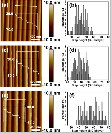
Figure 2. AFM topography 2 × 2 µm2 images and histograms of the statistic step heights for the as-grown 4H-SiC epilayers (a) and (b), graphene samples grown at 1800 °C for 16 min (c) and (d)) and for 30 min (e) and (f), respectively. The step height profiles of the indicated lines with a dimension of 1 µm are shown in the insets of images (a), (c) and (e). The step heights were obtained from several AFM topography images of each sample.
Download figure:
Standard image High-resolution imageThe number of graphene layers for each sample was first evaluated by the reflectance mapping in combination with corresponding Raman mapping and micro-Raman spectra [23, 24]. For the sample grown at 1800 °C for 16 min, the reflectance results shown in figures 3(a) and (b) indicate that the graphene layer number is around 1–2 layers, according to the previously reported method [23]. The Raman maps of the peak positions and full width at half maximum (FWHM) of the 2D peaks are displayed in figures 3(c) and (d), which are measured on the same region as the reflectance map. The 2D peak at 2735 cm−1 collected on the position 1 exhibits a single Lorentzian shape with a FWHM of ~45 cm−1, suggesting monolayer graphene. While the 2D peak measured on position 2 exhibits asymmetric shape and shows an obvious blueshift to 2744 cm−1 with an increase of FWHM to ~55 cm−1, indicating the feature of bilayer graphene. The shift of the 2D peak could be due to the variations of the electronic band structure with the increasing number of graphene layer [25]. The larger FWHM is related to the appearance structure (multiple bands) within the 2D peak in the case of multilayer graphene [26]. Therefore, the reflectance map and Raman spectra indicate that the red (1) and yellow region (2) are covered with monolayer and bilayer graphene, respectively.
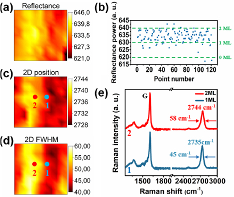
Figure 3. (a) 3 × 3 µm2 reflectance map on the sample grown on the 4H-SiC epilayer at 1800 °C for 16 min. (b) Distribution of the reflected laser intensity for all of data points in (a). (c) and (d) 3 × 3 µm2 Raman maps of the peak positions and FWHM of the 2D peaks, which are generated from the Raman spectra measured on the same region as the reflectance map. (e) Raman spectra collected at the labeled positions in (c) and (d).
Download figure:
Standard image High-resolution imageFigure 4 shows the reflectance and Raman results of the graphene sample grown on the 4H-SiC epilayer at 1800 °C for 30 min. The reflectance map in figure 4(a) shows quite uniform contrast and the reflected laser intensities in figure 4(b) are mostly distributed around bilayer graphene. Some regions with higher reflectance can be observed as well, suggesting that trilayer-graphene inclusions presumably also exist. Raman maps of the peak positions and FWHM of the 2D peaks in figures 3(c) and (d) show similar results as the former graphene sample, in which Raman spectra demonstrates the presence of monolayer and bilayer graphene. Consequently, this sample contains dominant bilayer graphene with small area of monolayer graphene, and trilayer graphene cannot be precluded.
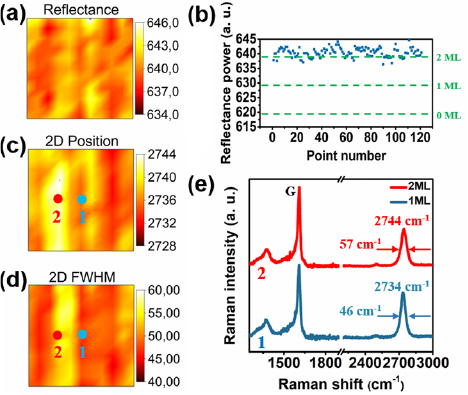
Figure 4. (a) 3 × 3 µm2 reflectance map on the sample grown on the 4H-SiC epilayer at 1800 °C for 30 min. (b) Distribution of the reflected laser intensity for all of data points in (a). (c) and (d) 3 × 3 µm2 Raman maps of the peak positions and FWHM of the 2D peaks, which are generated from the Raman spectra measured on the same region as the reflectance map. (e) Raman spectra collected at the labeled positions in (c) and (d).
Download figure:
Standard image High-resolution imageIn addition, the Raman spectra of both graphene samples contain two broad bands centered at ~1365 cm−1and ~1600 cm−1, as seen in figures 3(e) and 4(e). These broad band features are attributed to the spectrum of the buffer layer underlying the graphene on hexagonal SiC substrates [27]. The D peak, which is associated with defects, would overlap the broad band since it is always peaking at around ~1350–1355 cm−1 [26]. Therefore, the D peak might also contribute to the low-energy band at ~1365 cm−1, but its negligible intensity suggest a good crystalline quality of the grown graphene layers.
LEEM measurements were used to further confirm the layer numbers of graphene grown on the step-structured surface of 4H-SiC epilayer. Herein, the AFM phase images were simultaneously measured with the AFM topography images for graphene samples shown in figures 2(c) and (e). For the graphene sample grown on the 4H-SiC epilayer at 1800 °C for 16 min, the AFM phase image shows bright and dark contrasts, which correspond to the terraces and facets (figures 5(a) and (b)), respectively. As shown in figure 5(c), the widths of bright and dark contrasts are ~150 nm and ~50 nm, respectively. These values are consistent with the average widths of the terrace and facet shown in the step profile. This indicates that the terraces are homogeneously covered with monolayer graphene, although we observe few bilayer graphene stripes covered some terraces. The number of graphene layers are confirmed by the number of dips in electron reflectivity curves (figure 5(d)) [28]. The structural quality of graphene layers is characterized by µ-LEED measurements. The µ-LEED pattern in figure 5(e) measured on the monolayer graphene region displays (1 × 1) graphene spots and surrounding (6 √3 × 6 √3) R30° buffer layer spots [29]. Such quite sharp graphene spots suggest a good crystalline quality of graphene layer. Due to the inclined step facets, electrons reflected/diffracted from such an edge do not contribute to the LEEM signal and it is impossible to judge the graphene coverage on the facets. We will employ STM to further study the properties of graphene grown on step facets below.

Figure 5. AFM phase images (a) and (f), the step profiles (b) and (g) collected from yellow lines, and LEEM images (c) and (h) of the graphene samples grown on the 4H-SiC epilayer at 1800 °C for 16 min (a)–(e) and 30 min (f)–(j), respectively. Both LEEM images (field of view = 5 µm) were measured with an electron energy of 5.3 eV. (d) and (i) The electron reflectivity curves collected from the colorfully labeled regions in (c) and (h), respectively. (e) and (j) The µ-LEED patterns measured at 45.0 eV from the monolayer region in (c) and the bilayer region in (h), respectively. A probing area of 500–1000 nm was used during µ-LEED measurements.
Download figure:
Standard image High-resolution imageFor the sample grown on the 4H-SiC epilayer at 1800 °C for 30 min, the AFM phase image also exhibits the stripe-structured contrast between the terraces and step edges (figures 5(f) and (g)). The step profile shows that the width of the terraces is around 200 nm and the width of step facets around 80 nm, which are larger than those of the sample grown for 16 min. As discussed above, the longer annealing results in larger steps due to subsequent step bunching (figure 2). By comparison of AFM and LEEM results, we found that the terraces were covered by monolayer or bilayer graphene while trilayer graphene has started to form at some step edges. The LEED pattern in figure 5(j) exhibits quite sharp (1 × 1) graphene diffraction spots as well, revealing a high-quality crystalline graphene.
In order to reveal the true topography of the step edge facets, we have employed STM to study the first graphene sample (grown at 1800 °C for 16 min) as representative. A typical surface survey STM micrograph shown in figure 6(a) demonstrates two arbitrary chosen ( ) step facets. Both facets are about 13–15 nm high and 30–35 nm wide, which gives an incline angle of 23–25 degrees. These structural parameters do not vary significantly at different parts of the sample. Most importantly, we found that these angles are independent of the step heights and are similar to the angles which have been reported for faceted sidewalls produced by lithography either along [
 ] or [
 ] direction of the SiC [3–5, 9, 15, 18, 30].
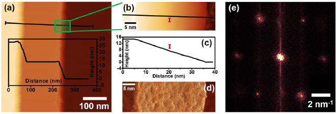
Figure 6. STM view of step facets and graphene on them. (a) A survey STM image of the sample surface. The inset shows the height profile along the black line above. It setpoint = 600 pA, Vbias = 1.25 V; scan size is 500 nm. (b) Shows a close-up STM image of a step edge highlighted in (a) with a white box. It = 300 pA, Vbias = 0.008 V; image size is 45(h) × 15(v) nm. (c) is a height profile along the black line in (b). (d) Shows the tunneling current channel of the same scan as in (b). Note that the topographic information is not preserved in It channel. (e) Shows a fast Fourier transform from a square area arbitrarily chosen on the step facet. Only six graphene spots are visible, suggesting the absence of other long-range symmetry.
Download figure:
Standard image High-resolution imageFigure 6(b) demonstrates a high-resolution STM micrograph of the step facet in figure 6(a), as sketched with green lines. Due to the considerable height variation along the scanning direction, it is difficult to resolve atomic structure of the step in the topography (Z-channel) channel of the STM, although atomic arrangement of the top and bottom terraces is visible in figure 6(b). Moreover, it is worthy to note that no supporting structure in the form of, for instance mini-terraces or 'washboard' structure has been observed. In general, a low density of mini-terraces is favorable for the observation of ballistic transport [5]. The height profile across the step facet, shown in figure 6(c) is a slightly buckled smooth curve, with quite a few steps or micro terraces whatsoever. This allows us to conclude that graphene is most likely freestanding on the step edges rather than tightly bound to the underlying substrate.
Figure 6(d) shows the same micrograph as in figure 6(b), taken using tunneling current (It) channel of the STM. Despite the topographic information is not preserved in It-channel, the observed features may become enhanced, which was the case for our study. It is clearly seen that the graphene overlayer almost perfectly flat on the top and bottom terraces (left and right, darker, parts of the image in figure 6(d)) becomes buckled on the step facet (center of the image). Its atomic arrangement, however, remains intact or nearly intact. Figure 6(e) shows a fast Fourier transform from a square area arbitrarily chosen on the step facet in figure 6(d). Only six graphene spots are visible, suggesting the absence of other long-range symmetry.
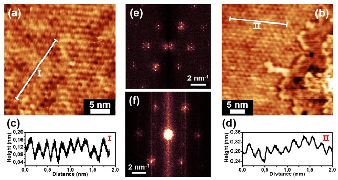
It is instructive to consider the sample structure not only on the step facet, but around it. Figures 7(a) and (b) shows the high-resolution STM micrographs taken respectively below and above the step facet discussed in figures 6(b) and (d). Figure 7(a) depicts a honeycomb-lattice with an additional trigonal corrugation pattern with approximately 2 nm period. The amplitude of the corrugation deduced from the respective height profile (figure 7(c)) reaches 0.12 nm indicating a strong interface interaction. This leads to a conclusion that the 'bottom' terrace is covered with buffer layer rather than with freestanding graphene. The Fast Fourier transform of figure 7(a) shows a set of principal spots, surrounded by six satellite spots (figure 7(e)), which further confirm the presence of buffer layer. This conclusion is also supported by the LEED results discussed above.
Figure 7. High-resolution STM micrographs taken respectively below and above the step facets shown in figure 6(b). (a) High-resolution STM micrograph of the 'bottom' terrace. It setpoint = 300 pA, Vbias = 0.008 V; scan size is 30 nm. (b) High-resolution STM micrograph of the 'top' terrace. It setpoint = 300 pA, Vbias = 0.005 V; scan size is 40 nm. (c) Is the height profile along the white line in (a) and (d) is a similar height profile for (b). (e) and (f) Are fast Fourier transforms of (a) and (b), respectively.
Download figure:
Standard image High-resolution image
As for the 'top' terrace shown in figure 7(b), this one consists of two distinct regions. In the biggest one, which occupies the left-center part of the micrograph, one still resolves the same corrugation network as shown in figure 7(a). The corrugation amplitude does not exceed 0.03 nm, although the periodicity of the corrugation network is still around 2 nm (figure 7(d)). This could be ascribed to that this region may be bilayer or even trilayer graphene, which would reduce the corrugation. The rightmost part of the image is visibly more buckled and irregularly corrugated, however, the graphene overlayer is intact on it and is resolved even better than in the rest of the image. The pattern of fast Fourier transform of this image is presented in figure 7(f). Although the satellite spots are not as clear as in pattern in figure 7(e), one still observes this characteristic spot arrangement. Therefore, one may assume that the 'top' terrace is also covered mostly with buffer layer on SiC, with some small fraction of graphene in the direct vicinity of the step edge.
Conclusions
In summary, we report a novel pattern-free approach to directly grow free-standing GNRs on off-oriented 4H-SiC epilayers without any patterning or lithography. First, the 4H-SiC epilayers with well-defined bunched steps were intentionally grown on 4 degree off-axis 4H-SiC substrates by a sublimation epitaxy technique. Then, the free-standing GNRs were grown on the step-structured 4H-SiC epilayers by thermal decomposition of SiC. Micro-Raman spectroscopy and LEEM measurements confirmed the number of graphene layers on the terraces of SiC. STM studies reveal that the inclined step facets are about 13–15 nm high and 30–35 nm wide, which gives an incline angle of 23–25 degrees. These angles are independent of the step heights and are similar to the angles reported for faceted sidewalls produced by lithography. LEEM and LEED results showed that the terraces are mainly covered by monolayer graphene and the buffer layer underneath it. STM images and the analysis of their Fourier transform patterns suggest that on the facets, in-between terraces, graphene is strongly buckled and appears to be largely decoupled from the surface.
Acknowledgment
This work was supported by The Swedish Research Council (Vetenskapsrådet, Grants Nos. 621-2014-5461 and 2018-04670), The Swedish Research Council for Environment, Agricultural Sciences and Spatial Planning (FORMAS, Grant No. 2016-00559), The Swedish Foundation for International Cooperation in Research and Higher Education (STINT, Grant No. CH2016-6722), The ÅForsk foundation (Grant No. 16-399), The Stiftelsen Olle Engkvist Byggmästare (Grant No. 189-0243), and The Swedish Foundation for Strategic Research (SSF, Grants GMT14-0077, SSF RMA15-0024).
Notes
The authors declare no competing financial interest.