
Abstract
Ga(In)SbBi alloys grown by molecular-beam epitaxy on GaSb substrates with up to 5.5% In and 1.8% Bi were studied by temperature- and power-dependent photoluminescence (PL) and compared to previous photoreflectance (PR) results. High energy and low energy PL peaks were observed and attributed respectively to Ga(In)SbBi bandgap-related emission and native acceptor-related emission. For GaSbBi below 100 K, the HE peak is at slightly lower energy than the bandgap determined from PR, indicating carrier localization. This phenomenon is significantly weaker in PL of GaInSbBi alloys, suggesting that the presence of indium improves the optical quality over that of GaSbBi.
Export citation and abstract BibTeX RIS

Original content from this work may be used under the terms of the Creative Commons Attribution 3.0 licence. Any further distribution of this work must maintain attribution to the author(s) and the title of the work, journal citation and DOI.
1. Introduction
Dilute III–V bismides are a very important class of highly mismatched alloys (HMAs) which have attracted great interest in recent years due to their unusual fundamental properties (including strong bandgap bowing, carrier localization at low temperatures, etc), and their potential in the development of various optoelectronic devices operating in the mid-infrared spectral region [1–4]. It has been shown that a small quantity of Bi added to host GaSb material reduces the bandgap with a rate of ~30–36 meV/%Bi or 210 meV per 0.01 Å−1 change in lattice parameter [5–8]. Such bandgap reduction is caused by the downward shift of the conduction band due to Bi 6s states and the valence band anticrossing effect (VBAC) [9], in which Bi 6p states interact with GaSb valence bands, shifting the valence band maximum (VBM) upward [8].
Among dilute bismides grown on GaSb substrate, GaSbBi alloys were investigated relatively intensively in recent years [5–8, 10–15]. However, only sporadic reports of GaInSbBi can be found in the literature [16–18]. Because the valence band offset between InSb and GaSb is negligible [19], In and Bi elements both reduce the bandgap of GaSb; In incorporation causes a downward shift of the conduction band minimum (CBM) and enhances the electron confinement when the material is used as a quantum well, while Bi lowers the CBM and simultaneously shifts the VBM up in energy [5, 8], enhancing both electron and hole confinement in the case of quantum well. Apart from reducing the bandgap energy, diluted amounts of In and Bi in GaSb increase the lattice parameter because InSb and GaBi have lattice constant greater than that of GaSb [5, 19]. In this context, GaInSbBi quaternary alloys offer flexibility in the bandgap and band offset tuning in the mid-infrared in addition to what is already available from conventional III–V semiconductor alloys and dilute nitride antimonides [20, 21]. Especially, GaSb-based dilute bismide alloys may offer means of overcoming the limitations of GaInAsSb alloys for achieving high continuous wave output power laser diodes at wavelengths beyond 2.7 µm at room temperature by improving the quantum confinement potential for both electrons and holes, and hence improving a material gain in laser quantum wells [15, 22, 23].
In this paper, the temperature dependence and power dependence of emission studies of GaInSbBi quaternary alloys grown by molecular beam epitaxy (MBE) are presented. The optical properties of the alloys are studied using photoluminescence spectroscopy. Investigations are performed for GaInSbBi alloys with similar Bi content and In concentration ranging from 0 to 5.5%. It is clearly shown that incorporation of In into GaSbBi improves optical properties.
2. Experimental details
The GaInSbBi epilayers used for these studies were grown by solid-source MBE on un-doped (0 0 1) GaSb substrates at a nominal growth rate of 1.0 µm h−1. The sources and substrate preparation procedures are described elsewhere [5]. For each substrate, the oxide was removed under an incident Sb flux at approximately 550 °C and then a 100 nm GaSb buffer layer was grown at 500 °C. Thereafter, the substrate was cooled to 275 °C and the GaInSbBi epilayer was grown. A determination of Ga:In ratio was done by growing a calibration layer of GaInSb with a thickness of ~100 nm. This layer was grown before the growth of GaInSbBi. Each GaInSbBi layer was grown using the same Ga and In fluxes as for the GaInSb layer, and the thickness of each GaInSbBi layer was ~300 nm. More details about the growth and composition determination using x-ray diffraction of the GaInSbBi samples can be found in [18].
The temperature dependent and laser power dependent photoluminescence (PL) was performed using a single grating 0.3 m focal length monochromator, along with a thermo-electrically cooled, InGaAs pin photodiode. A semiconductor laser (532 nm line and 80 mW) was used as an excitation source. The laser beam was focused onto the sample to a diameter of ~0.1 mm, and the power of the laser beam was tuned using a neutral density filter. Samples were mounted on a cold finger in a helium closed-cycle refrigerator coupled with a programmable temperature controller, allowing measurements in the 15 to 290 K temperature range
3. Results and discussion
Figure 1 shows temperature dependent PL spectra of GaSb0.984Bi0.016, Ga0.967In0.033Sb0.982Bi0.018, and Ga0.945In0.055 Sb0.987Bi0.013 samples, taken in the temperature range from 15 K to 290 K and plotted with temperature increments of 20 K, but the first interval is 15 K, from15 K to 30 K. The excitation power used to obtain PL data was 80 mW. Additionally, the PL spectra are normalized to the peak maximum, to show the temperature dependence of the peak position. The PL peak, observed at 0.79 eV at temperatures below 100 K in GaInSbBi, is associated with a bound-exciton recombination in the GaSb buffer and/or substrate [24, 25]. Below this peak, strong emission from GaSbBi (figure 1(a)) or GaInSbBi (figures 1(b) and (c)) is observed.
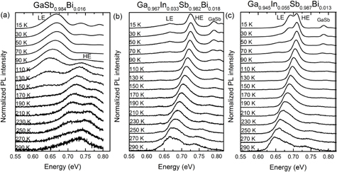
Figure 1. Temperature dependence of PL spectra for (a) GaSb0.984Bi0.016, (b) Ga0.967In0.033Sb0.982Bi0.018, and (c) Ga0.945In0.055Sb0.987Bi0.013. All the spectra are normalized to the peak maximum. The peaks observed at 0.79 eV and 0.81 eV at 15 K, correspond to bound-exciton and free exciton recombinations, respectively in the GaSb substrate or buffer [24, 25]. Reproduced from [24] © IOP Publishing Ltd. All rights reserved. Reprinted from [25] with permission from Elsevier. The spectra were collected at the excitation power of 80 mW.
Download figure:
Standard image High-resolution imageThe epilayer-related emission consists of two PL peaks: a low-energy (LE) and a high-energy (HE) peak. The LE peak is observed at low temperatures below 90 K in the case of GaInSbBi and below 150 K in the case of GaSbBi alloys. The spectral position of the LE peak indicates that it is a defect-related emission in the epilayer and such localized emission is usually observed in narrow gap HMAs [7, 26]. The second PL peak observed in the studied samples is the HE peak. At 15 K temperature this peak is attributed to an exciton localization, however at temperatures above 100 K the HE peak is attributed to a band-to-band recombination in the epilayers, i.e. a recombination between delocalized states. The character of the HE peak is deduced from the comparison of the PL peak position with the bandgap determined from photoreflectance (PR) measurements in our previous studies on GaInSbBi layers [18]. Additionally, the HE peak has an asymmetric shape, which is typical for narrow gap semiconductors with significantly different effective masses for electrons and heavy holes. This can be attributed to a contribution of band-to band emission. Similar behaviour of the PL peak shape was observed in InNAsSb layers [27]. Because of the narrow energy gap of GaInSbBi alloys, the free carrier emission starts to be important above 100 K and cannot be neglected.
Figure 2 shows the analysis of the spectral position of PL peaks for the GaSb0.984Bi0.016, Ga0.967In0.033Sb0.982Bi0.018, and Ga0.945In0.055Sb0.987Bi0.013 samples with the bandgap determined through PR measurements [18]. The overlap of the closed squares and open circles above 100 K confirms that the HE peak is associated with the bandgap-related emission. At 15 K the HE peak is attributed to an exciton localization. For the sample with In = 0% the difference in energy between the band gap value and spectral position of the HE peak is ~0.014 eV (see figure 2(a)). After incorporation of In atoms it is clearly visible that the localization is weaker or even negligible (see figures 2(b) and (c)). All the studied samples have a similar Bi content. Therefore, it can be determined that the energy difference between LE and HE peaks decreases in the presence of In.

Figure 2. Energies of LE and HE PL peak maxima, obtained from peak fitting (open circles) and the bandgap determined from PR measurements (closed squares) (a) GaSb0.984Bi0.016 (results taken from [7]), (b) Ga0.967In0.033Sb0.982Bi0.018, and (c) Ga0.945In0.055Sb0.987Bi0.013. (a) Reproduced with permission [7]. (b), (c) Reprinted from [18]. with the permission of AIP Publishing.
Download figure:
Standard image High-resolution imageIn order to determine the character of the PL emission, we performed PL measurements at various excitation powers and temperatures. Figure 3 shows example PL spectra collected from the Ga0.945In0.055Sb0.987Bi0.013 layer in the excitation power range of 2.5–80 mW at three different temperatures. At 15 K the position of the LE peak shifts toward lower energies with decreasing excitation power, indicating the localized nature of this peak (figure 3(a)). At temperatures higher than 100 K the LE peak disappeared; only the HE peak was visible and a lack of spectral shift of this peak with changing the excitation power confirms the bandgap-related nature of this emission (figures 3(b) and (c)). A similar behavior of PL spectra with increasing excitation power was observed in the Ga0.967In0.033Sb0.982Bi0.018 sample and also in ternary GaSbBi alloys [7].
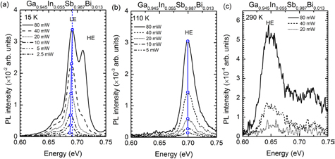
Figure 3. PL spectra for a Ga0.945In0.055Sb0.987Bi0.013 layer at various excitation powers at (a) 15 K, (b) 110 K and (c) 290 K. A vertical dashed blue line denotes the position of the LE peak at 80 mW excitation power. Solid blue lines indicate the shift of the peak maximum with changing the excitation power.
Download figure:
Standard image High-resolution imageIt is well established that the PL intensity IPL increases with the excitation power Iex, and the relation can be expressed as

where the exponent α represents the type of recombination mechanism. For excitation laser light with energy exceeding the bandgap energy, the exponent α is generally between 1 and 2. α = 1 for the purely excitonic emission (free- and bound-exciton emission), and α is less than 1 for free-to-bound and donor–acceptor pair recombination. α equals 2 indicates a band to band recombination [28]. Analysis of the Ga0.967In0.033Sb0.982Bi0.018 (figure 4(a)) yields a PL intensity versus pump power α coefficient of 1.5 at 290 K and α of 0.7 at 15 K. Similarly, analysis of the Ga0.945In0.055Sb0.987Bi0.013 (figure 4(b)) yields α of 1.6 at 290 K and α of 0.85 at 15 K. At low temperature the α is less than 1, suggesting a free-to-bound and/or donor–acceptor pair recombination. The excitons tend to be localized and cannot reach nonradiative recombination centers. In this case free excitons can be efficiently trapped by local potentials related to fluctuations of Bi and In [29, 30]. As temperature is increased up to room temperature, the character of the PL changes substantially (the α coefficient is bigger than 1.5). At this temperature limit, the excitons are free due to a thermal activation and coexist with free carriers. These can now reach nonradiative recombination centers. Consequently a nonradiative recombination dominates and reduces the number of excitons which could recombine radiatively. As a result, the PL intensity becomes weaker at the same level of excitation. However, an observation of quite strong PL up to room temperature means that the concentration of native defects (non-radiative centers) is relatively low for these alloys.

Figure 4. PL intensity of GaInSbBi samples measured at 15 K, 110 K and 290 K with different excitation power. Lines show fits to the relation (1). (a) Ga0.967In0.033Sb0.982Bi0.018, (b) Ga0.945In0.055Sb0.987Bi0.013.
Download figure:
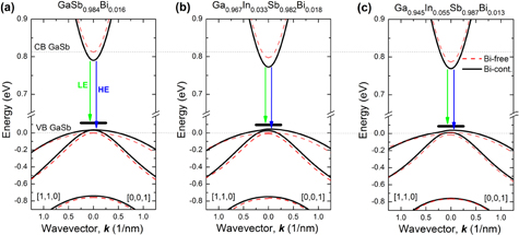
Standard image High-resolution imageTo explain the nature of LE emission the electronic band structure has been calculated within the 14-band kp model [23] with the Bi-related shift of conduction and valence band anticrossing (VBAC) parameters tuned to obtain agreement with experimental data [31]. The VBAC model coupling parameter was found to be ~1.5 eV. The compressive strain in Ga(In)AsBi layers has been taken into account according to the Bir–Pikus theory as shown in detail in [22]. Figure 5 shows the dispersion of the conduction and valence bands for the three Ga(In)SbBi samples near the center of the Brillouin zone (thick solid lines) together with the conduction and valence band dispersions in Ga(In)Sb as the reference (red dashed lines). First it is clearly visible that the incorporation of Bi atoms into Ga(In)Sb host leads to type I bandgap alignment between GaSb and Ga(In)SbBi, which is very important for applications of this alloy in GaSb-based quantum wells dedicated for light emitters. Second it is observed that the bandgap calculated for the three alloys is very consistent with the spectral position of the HE peak in PL spectra while the spectral position of the LE peak can be explained by the radiative recombination between the conduction band and an acceptor level, which is observed at very similar energy. In general such a situation is expected for deep levels and therefore the LE emission is attributed to free-to-bound (deep acceptor) recombination, which is consistent with the power dependent PL measurements and the analysis of the α parameter for the LE peak. This conclusion is also consistent with our previous studies for GaSbBi alloys of various Bi concentrations [7].
Figure 5. Electronic band structure of (a) GaSb0.984Bi0.016, (b) Ga0.967In0.033Sb0.982Bi0.018, and (c) Ga0.945In0.055Sb0.987Bi0.013 near the center of the Brillouin zone (thick solid lines) together with the electronic band structure of Bi-free host as the reference (red dashed lines). The position of the deep acceptor level is established on the basis of the LE peak position in PL spectra.
Download figure:
Standard image High-resolution image
Comparing PL spectra for In-free and In-containing samples, we conclude that indium improves optical properties in this material system: the contribution of the LE peak to the PL spectrum is smaller, the thermal quenching of the HE peak is weaker, and the broadening of the HE peak is smaller for In-containing samples. Therefore we are fully convinced that this alloy is very promising for applications in light emitters.
4. Conclusions
In summary, LE and HE emissions from GaInSbBi layers have been identified in PL spectra. The comparison of the HE peak position with the results obtained from photoreflectance measurements, and the asymmetric shape of the HE peak indicates it is due to bandgap-related emission. At low temperatures, the LE peak is observed and it is attributed to defect-related emission. The energy separation between HE and LE peak decreases with increasing In concentration. Additionally, at low temperatures the HE peak for GaSbBi is up to 0.014 eV below the bandgap determined by PR as a result of carrier localization. The localization energy is significantly reduced for the GaInSbBi alloys, suggesting the presence of indium improves the optical quality over that of GaSbBi alloys.
Acknowledgments
This work was performed within the grant of the National Science Centre, Poland (Grant No. 2014/13/D/ST3/01947). In addition, MG acknowledges financial support from the NCN Poland (Grant No. 2013/10/E/ST3/00520). JK acknowledges financial support from the NCN Poland (Grant No. 2015/17/N/ST3/02286). TDV acknowledges financial support from the Engineering and Physical Sciences Research Council (EPSRC) (Grant No. EP/G004447/2).