

Abstract
Inspired by an innovative sensing philosophy, a light-weight nanocomposite sensor made of a hybrid of carbon black (CB)/polyvinylidene fluoride (PVDF) has been developed. The nanoscalar architecture and percolation characteristics of the hybrid were optimized in order to fulfil the in situ acquisition of dynamic elastic disturbance from low-frequency vibration to high-frequency ultrasonic waves. Dynamic particulate motion induced by elastic disturbance modulates the infrastructure of the CB conductive network in the sensor, with the introduction of the tunneling effect, leading to dynamic alteration in the piezoresistivity measured by the sensor. Electrical analysis, morphological characterization, and static/dynamic electromechanical response interrogation were implemented to advance our insight into the sensing mechanism of the sensor, and meanwhile facilitate understanding of the optimal percolation threshold. At the optimal threshold (∼6.5 wt%), the sensor exhibits high fidelity, a fast response, and high sensitivity to ultrafast elastic disturbance (in an ultrasonic regime up to 400 kHz), yet with an ultralow magnitude (on the order of micrometers). The performance of the sensor was evaluated against a conventional strain gauge and piezoelectric transducer, showing excellent coincidence, yet a much greater gauge factor and frequency-independent piezoresistive behavior. Coatable on a structure and deployable in a large quantity to form a dense sensor network, this nanocomposite sensor has blazed a trail for implementing in situ sensing for vibration- or ultrasonic-wave-based structural health monitoring, by striking a compromise between 'sensing cost' and 'sensing effectiveness'.
Export citation and abstract BibTeX RIS
1. Introduction
Conductive polymer composites (CPCs), a prevailing modality of burgeoning nanocomposites, have been increasingly explored for the development of new functional and structural materials, transducers, antistatic devices, and electromagnetic shielding [1–4]. The nanofillers of CPCs can be diverse, as typified by carbon nanotubes (CNTs) [1, 2, 5, 6], carbon black (CB) [7], carbon fibers [8], and graphene [9], to name a few. The nanoscale of the nanofillers allows them to be dispersed in polymer matrices uniformly, and the coalescence between the nanofillers and polymers introduces some appealing and unique material features, such as low density, desired flexibility, easy shape tailorability, chemical stability, and favorable electrical-mechanical performance. Of particular recent research interest is the use of CPCs to attempt innovative sensors [1, 2, 10–26]. CPC-based sensors are demonstrably capable of perceiving structural or ambient changes with the desired sensitivity and accuracy, with successful paradigms including the detection of gas leakages and content [19, 20, 22–26], the measurement of static or quasi-static strains [1, 2, 13–18], the acquisition of dynamic responses [7, 21], and the detection of damage [10–12].
Against this backdrop, a great deal of effort has been directed towards the development of CPC-based piezoresistive strain sensors for measuring static (or quasi-static) deformation [17, 18], on whose basis a diversity of applications—and damage detection in particular—can be implemented. The cardinal premise for the use of such sensors for damage detection resides in the fact that damage in a structure to which the sensor is adhered can amend the electrical conductivity formed by nanofillers in sensors. Representatively, a CPC-based piezoresistive sensor composed of CNTs and polyvinylidene fluoride (PVDF) was prepared with various CNT concentrations [13, 14]. The stability and sensitivity of the sensor for strain signal acquisition, along with its susceptibility to ambient temperature, were evaluated rigorously. In another example, multi-walled CNT thin films were fabricated by a layer-by-layer (LbL) technique [27]. The responses of the thin films to various stimuli were investigated, whereby a two-dimensional mapping of the conductivity of the CNT thin films was constructed. The results are conducive to the development of a novel sensing skin. As an extension of the above work, CNT thin films were spray-deposited directly on a glass fiber composite laminate [28], and the spatially distributed electrical conductivity of the films was monitored. Using a benchmarking process against the voltage acquired when the laminate is in its intact status, the location and severity of low-velocity-impact-induced damage in the laminate were ascertained via an electrical impedance tomography algorithm. Compared with single-phase rigid ceramic sensing blocks (e.g., lead zirconate titanate (PZT)) or conventional metallic foil-based strain gauges, CPC-based piezoresistive strain sensors have been demonstrated to be more sensitive to material deformation, with additional merits such as enhanced measurement repeatability [13, 14, 27, 28].
Though effective in detecting the existence of damage, most CPC-based piezoresistive sensors, by measuring changes caused by damage in electrical resistance (ER), are confronted by inherent bottlenecks, including:
- i.The change in ER, measured by a pair of electrodes, is a global indicator for reflecting holistic material properties between the two electrodes, and therefore it offers limited information at a qualitative level—likely indicating the existence of damage beneath the sensor only. This is because the damage outside the coverage of a sensor would not alter the ER measured by that sensor.
- ii.Even with extended coverage, a sensor is still unwieldy in spatially locating damage beneath it, let alone in its use for the quantitative assessment of damage (including location and severity parameters). This is because the measured ER change is a uniform value across two electrodes, regardless of the discrepancy in location and the severity of different damage events.
- iii.Last but not least, most CPC-based sensors are capable of perceiving a relatively large amount of material deformation (on the order of millimeters) when the material undergoes a static or quasi-static (a few hertz) load, because only when the amount of material deformation is to such a degree can it introduce conspicuous change to the conductive networks formed by the nanofillers in the sensors. This, however, is obviously not the case for guided ultrasonic waves (GUWs)—GUWs usually feature a loading/unloading process with an ultralow magnitude (on the order of micrometers), yet in an ultrasonic frequency regime.
Restricted by these factors, the majority of existing CPC-based sensors, by exploring the changes in the conductive networks formed by nanofillers, may not accommodate the needs of quantitative damage detection, in which not only the existence of damage but also its location and severity are expected to be evaluated—although CPC-based sensors hold promise in the implementation of in situ signal acquisition.
Motivated by this and enabled by recent advances in nanotechnology, sensor techniques, and electronic packaging, a nano-engineered, lightweight CPC-based nanocomposite sensor made of a CB and PVDF hybrid was developed for the implementation of damage detection and structural health monitoring (SHM), which take advantage of dynamic elastic disturbance. Here, the dynamic elastic disturbance refers to either the global structural vibration signatures (e.g., eigen-frequencies, modal curvatures, mechanical impedance or damping [29]) or local GUW features (e.g., arrival time, phase delay, amplitude change) [30–38]. In the sensor, the PVDF serves as a matrix, while the CB nanofillers serve as reinforcement in order to form the conductive network optimally. Electrical analysis, morphological characterization, and static/dynamic electromechanical response investigation were performed, in order to advance our insight into the tunneling effect in the formed conductive network when the sensor responds to dynamic elastic disturbance. An optimal percolation threshold for the CB network was ascertained in order to achieve favorable sensitivity to the dynamic signals from low-frequency vibration to high-frequency GUWs in the range of hundreds of kilohertz, yet with ultralow magnitude. To examine the correctness, sensitivity and accuracy of the fabricated nanocomposite sensor, captured vibration and GUW signals were compared with the counterpart signals acquired by conventional strain gauges and piezoelectric transducers. Coatable to a structure and deployable in large quantities to configure a dense sensor network, this light-weight nanocomposite sensor is conducive to in situ sensing for SHM.
2. Sensor fabrication and characterization
2.1. Material preparation
CB (N220, with an average particle diameter of 80 nm, supplied by the CABOT Corporation) was chosen as the nanofiller, while PVDF (Kynar k721, with a density of 1.74 g cm−3 and a melting point of ∼158 °C, supplied by ARKEMA) was chosen as the matrix to fabricate the nanocomposite hybrid. The rudimental consideration of using CB as the nanofiller and PVDF as the matrix lies in the fact that: (i) CB has a nanoscalar size and high specific surface area with PVDF, and compared with other nanofiller candidates such as CNTs, it features a much reduced amount of nanoparticle entanglement [39–41], beneficial to the formation of an even, stable and uniform conductive network; (ii) PVDF, a thermoplastic material with a higher elastic modulus, can present a faster response to dynamic change than traditional rubber-based piezoresistive materials (rubber bases often exhibiting complex time- and frequency-dependent viscoelastic properties, restricting them from being responsive to fast-change signals). This property of PVDF makes the hybrid highly responsive to dynamic elastic disturbance without marked hysteresis (to be demonstrated in a sequential experiment). In addition, PVDF possesses other merits including low-density, chemical inertness, thermal stability, easy processing, and flexibility [13, 14, 42]. Together, CB and PVDF endow the fabricated nanocomposite hybrid with enhanced sensitivity and a high-fidelity response to the dynamic changes applied to the formed conductive network.
A standard melt-mixing process was applied to disperse CB nanofillers into the PVDF in an internal mixer at 190 °C and 50 rpm for 0.5 h. A variety of mass ratios of CB nanofillers to PVDF in the hybrid, ranging from 5 to 30 wt%, were considered during preparation. The fabricated nanocomposite hybrid was immobilized between two steel plates and molded into films ∼200 μm in thickness, using a standard hot-pressing process in which each film was hot-pressed at 20 MPa and 190 °C for 10 min, and then cooled to room temperature at atmospheric pressure for another 60 min. Upon curing, the nanocomposite films were tailored into rectangular flakes, each measuring 15 mm × 10 mm (the thickness remained at ∼200 μm). To introduce electrodes into each flake and configure the sensor, each one was silver pasted using a dual-component (polymer/silver powder) adhesive (D05001, Beijing Emerging Technology Co. Ltd, China) with shielded cables. The ER of each sensor with silver-pasted electrodes was measured, and found to be similar to the intrinsic ER of a raw flake prior to electrode installation. Moreover, no discernible discrepancy could be observed in the measured ER using the sensors from the same batch. Both imply a good sensor fabrication process and the proper installation of electrodes. A sensor with two electrodes in its final fashion is photographed in figure 1. Small and light-weight, such a sensor can be produced in a single fabrication process, and deployed in a large quantity for configuring a sensor network.

Figure 1. A fabricated CB/PVDF nanocomposite sensor with two silver-pasted electrodes (front and back view).
Download figure:
Standard image High-resolution image2.2. Sensor characterization
2.2.1. Electrical analysis
To ascertain the conductivity of the fabricated nanocomposite hybrid at each CB weight ratio, the ER of each sensor was measured using a standard four-probe method with a semiconductor characterization system (4200-SCS, Keithley Instruments, Inc., Cleveland, Ohio, USA) at room temperature. With the ascertained ER (R), the electrical conductivity (denoted by σ) was defined by  where A and l are the effective area and length between the two electrodes of the sensor, respectively. The accordingly obtained average σ (Siemens per meter, S m−1) at representative CB weight ratios (5, 6.5, 8, 10, 20 and 30 wt%) are listed in table 1 and plotted in figure 2, both revealing that a dramatic change in the conductivity of the sensor takes place when the CB weight ratio is between 5 and 8 wt%, in which even a slight increase in the ratio can lead to a significant alteration in the conductivity of the sensor.
Table 1. Average conductivity (σ) of the fabricated CB/PVDF nanocomposite sensors.
| Contents of CB [wt%] | σ [S m−1] |
|---|---|
| 5 | 1.0 × 10⁻⁶ |
| 6.5 | 1.0 |
| 8 | 2.5 |
| 10 | 7.5 |
| 20 | 60 |
| 30 | 220 |
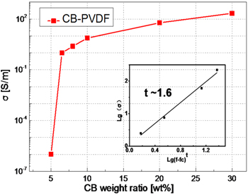
Figure 2. Average conductivity (σ) of the fabricated CB/PVDF nanocomposite sensors at different CB weight ratios (insert: log–log plot between σ and f pairs with linear fitting for the determination of the percolation threshold).
Download figure:
Standard image High-resolution imageIn both table 1 and figure 2, a marked increase in the electrical conductivity of the hybrid by six orders of magnitude can be observed from 5 wt% to 8 wt%, indicating the formation of a fully conductive CB network in the sensor at this particular CB weight ratio. On the basis of this, 5 ∼ 8 wt% of the CB content in the hybrid is deemed to be in the vicinity of the percolation threshold. The percolation threshold [43, 44] represents the transition of the hybrid from insulation to conduction, near which a slight increase in the CB content can give rise to a tremendous leap in the number of conductive paths formed by dispersed CB nanofillers, and consequently an abrupt increase in the conductivity of the sensor.
To ascertain the exact percolation threshold (denoted by fc) in the above-determined vicinity range of 5 ∼ 8 wt%, percolation theory was recalled [43, 44], in which σ of the sensor is defined as

where f signifies the fraction of conductive nanofillers (namely, the CB in this study) obtained from a series of measurements, fc is the percolation threshold to be determined, and t is the critical exponent depending on the nanofiller-formed conductive network. Using equation (1), fc was derived by applying a linear fitting on a series of measured σ and f pairs (as seen in the log–log plot in the insert of figure 2). Upon the linear fitting, fc and t of the fabricated nanocomposite hybrid were found to be ∼6.5 wt% and 1.6, respectively.
2.2.2. Morphological characterization
To gain an insight into the nanoscalar architecture of the formed CB conductive network when the sensor is subject to elastic disturbance, morphological characterization was implemented on the hybrid using scanning electron microscopy (SEM) (JSM-7500F, JEOL Ltd). First, the hybrid was fractured into small-sized samples (with a thickness of ∼200 μm for each) in liquid nitrogen. Sputter coating was applied on the cryofractured surface of each sample with a thin layer of gold. The obtained SEM images, at several representative CB weight ratios, are displayed in figure 3. It can be observed that CB nanofillers are dispersed in PVDF randomly and evenly throughout all the weight ratios, this implying a good fabrication process of the sensor. In particular, at the determined percolation threshold (∼6.5 wt%), figure 3(b), it is apparent that a substantial number of conductive paths have been created in the CB network owing to dramatically increased connections between the CB nanofillers and their aggregations. This yields an instantaneous transition from the insulative to conductive status of the sensor, compared with other cases in which the CB contents are below the percolation threshold (e.g., figure 3(a)). On the other hand, with higher CB weight contents beyond the percolation threshold (e.g., 20 wt% in figure 3(c), and 30 wt% in figure 3(d)), the CB network is densified and the CB nanofillers tend to be saturated in the matrix; no significant increase in conductivity can be measured in comparison with the case at ∼6.5 wt%. These observations from SEM images coincide with the percolation threshold of ∼6.5 wt% previously determined using the percolation theory.

Download figure:
Standard image High-resolution image
Figure 3. The nanoscalar structures of the fabricated CB/PVDF nanocomposite sensors at different CB weight ratios: (a) 5, (b) 6.5, (c) 20, and (d) 30 wt% (right: zoomed-in SEM image of the one on the left).
Download figure:
Standard image High-resolution imageX-ray diffraction (XRD) analysis was further carried out on the hybrid at room temperature on an XRD platform (X'Pert Pro, PANalytical, the Netherlands), in specular reflection mode (Cu Ka radiation [45]), and a scanning angle varying from 15° to 29° (with a scanning rate of 4° s−1). A typical XRD pattern at the determined percolation threshold (∼6.5 wt%) is displayed in figure 4(a).
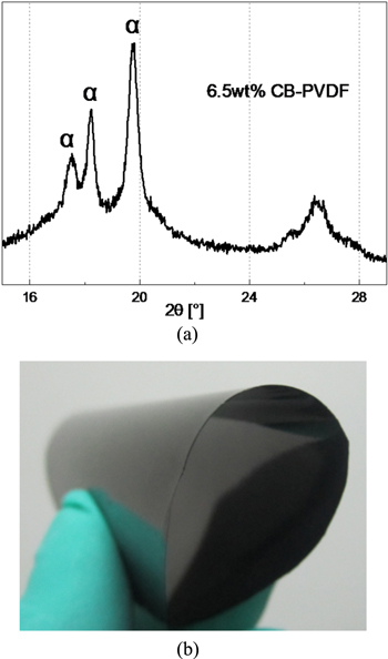
Figure 4. (a) The XRD pattern of the fabricated CB/PVDF nanocomposite sensors (2θ: scanning angle) and (b) the optical image of the hybrid CB/PVDF.
Download figure:
Standard image High-resolution imageThe XRD results argue that the fabricated hybrid possesses a characteristic pattern of α-crystals, and therefore features a nonpolar crystal structure. This speculation excludes the possibility that the piezoresistivity manifested by the sensors could originate from the PVDF matrix itself, rather than the CB conductive network induced by external dynamic elastic disturbance. This is because only a polar crystal (such as a β-crystal) can lead to piezoelectricity (as interpreted elsewhere [13, 14, 42, 43]). Furthermore, given that the fabricated sensor features a nonpolar crystal structure, the PVDF matrix in the hybrid would not cause prominent piezoelectricity, and once a change in the conductivity of the sensor is detected, it can be fully attributed to the consequence of the change in the CB conductive network caused by dynamic elastic disturbance (rather than the PVDF itself). In addition, the optical image, as seen in figure 4(b), reveals the good flexibility of the sensor, highlighting its capacity to adapt to non-flat structural surfaces—an intriguing merit of the sensor with practical engineering applications.
2.2.3. Static/dynamic electromechanical response interrogation
Taking a step further in order to advance understanding of the sensing mechanism when subjected to static and dynamic elastic disturbance, the static/dynamic electromechanical responses of the sensors at various CB weight ratios were evaluated with a dynamic mechanical testing platform (TA Q800, TA Instruments) and a semiconductor characterization system (4200-SCS, Keithley Instruments, Inc., Cleveland, Ohio, USA).
2.2.3.1. Static
Figure 5 shows the change in ratio of the measured ER of the sensors against static load-induced strain. For comparison, the change ratio of a typical metal-foil strain gauge is also included in the figure.

Figure 5. Change ratio of the measured ER of the fabricated CB/PVDF nanocomposite sensors at different CB weight ratios under static load.
Download figure:
Standard image High-resolution imageAs observed, at a given strain, the lower the CB weight ratio of the hybrid (between 6.5 ∼ 30 wt%), the higher the change ratio of the ER, and therefore the higher the gauge factor of the sensor. As discussed earlier, the nanoscalar architecture of CB nanofillers allows a high specific surface area of evenly dispersed nanofillers in the PVDF once a conductive network is formed, and this can advance the sensing sensitivity of the sensor to strain as a consequence of the breakage of the network and the introduction of the tunneling effect [15, 16, 27]. As demonstrated elsewhere [15, 16, 27, 46], the tunneling effect is dominant when the nanofiller or adjacent building block is in close proximity (on the order of several nanometers) but not in direct contact with the each other. In particular, when the strain is not to a significant degree (such as the low strain induced by ultrasounds), the tunneling effect is considered to be the key mechanism leading to the change in conductivity of the sensor.
A further increase in the CB content only densifies the conductive paths in a saturated conductive network, and a saturated network is not prone to be affected by further increases in strain (not giving rise to an increase in the gauge factor). Therefore, a higher CB content (such as 30 wt%) of the hybrid leads to a smaller change ratio of ER (therefore a lower gauge factor), compared with a lower CB content (such as 6.5 wt%). Using another means, this has corroborated the previously determined percolation threshold. By calculating the ratio of resistance change to strain, the gauge factor of the fabricated sensor was calculated to be 5.0 ± 0.6 (at ∼6.5 wt%)—much higher than that of a metal-foil strain gauge, which is usually ∼2 [15] (as seen in figure 5). The high gauge factor guarantees the superior sensitivity of the sensor to small strains in the case of GUWs (GUWs usually feature a weak magnitude on the order of several microstrains).
2.2.3.2. Dynamic
By extending the static loading in the above to dynamic loading using the same testing platform, the sensor was applied with a cyclic load windowed in ramp strain mode with a ramp rate of 1.0% per minute until reaching its maximum at 1.0%. As a representative result, the change ratio of ER measured by the sensor at the percolation threshold (∼6.5 wt%), when subjected to the applied cyclic load, is displayed in figure 6. This is done in order to observe high consistence between the response and the applied cyclic load without discernable hysteresis, asserting good dynamic stability and the desirable measurement repeatability of the sensor.
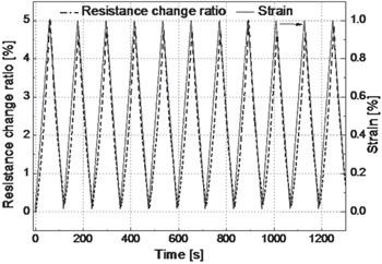
Figure 6. Electromechanical response of the fabricated CB/PVDF nanocomposite sensors in comparison with the applied cyclic load (at percolation threshold).
Download figure:
Standard image High-resolution imageVery importantly, the observed reversibility of the sensor response under a cyclic load corroborates the conclusion drawn earlier that under small strains (e.g., GUWs), the dominant sensing mechanism of the sensor is the tunneling effect among nanofillers, instead of the loss of contact or breakage of the conductive network. This is because the latter is inclined to induce an irreversible change in the ER measured by the sensor.
Both the static and dynamic electromechanical response interrogations have demonstrated that the fabricated sensor, at the determined percolation threshold, possesses a capacity to perceive material deformation under static or dynamic loads, with reversibility yet without hysteresis. This can be attributable to the tunneling effect, accompanied by the loss of contact between nanofillers not thought to be dominant—a property to be exploited for the acquisition of dynamic structural vibration and GUWs in what follows.
3. In situ acquisition of dynamic elastic disturbance
The feasibility, correctness, and sensitivity of the fabricated CB/PVDF nanocomposite sensors to perceive dynamic elastic disturbance was examined, ranging from low-frequency structural vibration to high-frequency GUWs. On the basis of previous material characterization, the sensor with a percolation threshold of ∼6.5 wt% was selected for the sake of its highest gauge factor. Light-weight and small, the sensor can be conveniently and quickly glued on the surface or embedded into a structure to implement in situ signal acquisition—without introducing obvious weight or volume penalty to the host structure.
3.1. Dedicated signal amplification and acquisition system
Owing to the weakness of the magnitude of elastic disturbance, and particularly that of the GUWs in a frequency range of kilo- or megahertz (GUW-induced elastic disturbance is usually on the order of several microstrains), the signals captured by the sensors are envisaged to be prone to contamination from ambient noise and uncertainties, and this, under most circumstances, leads to a low signal-to-noise ratio (SNR). To circumvent this, a self-contained signal amplification and acquisition system was developed, to be used in conjunction with the sensors. The system embraces a signal amplification module and a signal generation/acquisition module developed on a PXI (PCI extensions for instrumentation) bus platform (NI® PXIe-1071).
The amplification module integrates a Wheatstone bridge with resistors compatible to the ER of the selected sensor (the ER was ascertained via electrical analysis, detailed in section 2.2.1), an electronic amplifier circuit, a series of filters and a signal conversion unit (for converting the measured piezoresistivity to electrical voltage signals). The signal generation/acquisition module consists of an electromechanical shaker (B&K® 4809) for introducing vibration to a structure, a waveform generator (NI® PXIE-1071) for exciting GUWs via PZT wafers (Physik Instrumente Co., Ltd, PIC151; diameter: 9 mm; thickness: 0.5 mm), a linear power amplifier (Ciprian® US-TXP-3), and an oscilloscope (Agilent® DSO9064A). Using these two modules, the structural vibration and GUW signals were generated and then captured.
3.2. Low-frequency structural vibration
A cantilevered glass-fiber-epoxy composite beam (290 mm long, 38 mm wide and 2 mm thick) was prepared, to which a nanocomposite sensor and a strain gauge sensor (for comparison) were attached to the surface using an instant glue (Aron Alpha® HHI-11485). The central position of the sensor was measured 70 mm from the clamped end of the beam, as seen in figure 7. The shaker excited the beam through a point 270 mm from the clamped end, with a sinusoidal signal sweeping between 100 and 2000 Hz.

Figure 7. (a) Photograph and (b) schematic of the experimental set-up for the acquisition of the low-frequency vibration of a glass-fiber-epoxy composite beam (unit: mm).
Download figure:
Standard image High-resolution imageTo facilitate a better understanding of the signals captured by the sensor, bandpass filters were designed and applied to the raw signals, in order to screen measurement noise. All the captured signals were averaged 16 times to remove random noise and uncertainties. The signals, acquired at the three representative frequencies (100, 500 and 2000 Hz) are presented in figures 8(a) to (c), respectively, to observe good repeatability of the sensor response. Furthermore, the discrepancy in the signal phase between the responses acquired by the CB/PVDF sensor and the strain gauge is barely discerned in figure 8(c), from which it can be extrapolated that the hysteresis of the fabricated sensor, in response to a dynamic elastic disturbance up to 2000 Hz, is unperceivable. In a previous study, a rubber-based piezoresistive sensor was used to measure the piezoresistive response of a similar case, but to observe a certain delay in response to excitation; such delay generally increases with the frequency of applied pressure due to the intrinsic viscoelastic properties of rubber [21]. This echoes the previous justification pertaining to the selection of PVDF as the sensor matrix—the high elastic modulus of the PVDF drives the sensor to be responsive to dynamic disturbance without marked hysteresis.

Figure 8. Vibration signals captured by the fabricated CB/PVDF nanocomposite sensor (a) with different excitation magnitudes (at 100 Hz), (b) at 500 Hz and (c) and strain gauge sensor (at 2000 Hz) and (d) signal amplitudes with different excitation magnitudes (at 100 Hz and 2000 Hz).
Download figure:
Standard image High-resolution imageFurthermore, by adjusting the magnitude of excitation, the accordingly acquired signals, at 100 Hz and 2000 Hz, are compared in figure 8(d) and demonstrate a good linear correlation between excitation and response. This observation surmises an approximately linear response for the nanocomposite sensor to the dynamic elastic disturbance (up to the discussed frequency of 2000 Hz). In addition, the minute error bar in figure 8(d) accentuates the stability of the sensor in performing different measurements.
3.3. High-frequency GUWs
In the above, from the barely discerned discrepancy in phase between the responses acquired by CB/PVDF and the strain gauge, it can be extrapolated that the hysteresis of the fabricated sensor, in response to dynamic elastic disturbance up to 2000 Hz, is unperceivable. Subsequently, the performance of the sensor was examined in an ultrasonic regime. A glass-fiber-epoxy composite laminate panel (600 mm × 600 mm × 2 mm) was prepared, as shown in figure 9. To activate the GUWs in the panel, two PZT wafers, denoted by PZT1 and PZT2, respectively, were surface-mounted on the laminate with their respective locations specified in figure 9. Each PZT wafer served the dual-role of actuator and receiver, respectively, in terms of piezoelectricity. Eight nanocomposite sensors were glued to the surface of the laminate, on the same side of the laminate as the two PZT wafers, to form a sensor network with a coverage area of 300 × 300 mm2.

Figure 9. (a) Photograph and (b) schematic of the experimental set-up for the acquisition of high-frequency GUWs propagating in a glass-fiber-epoxy composite laminate panel (unit: mm).
Download figure:
Standard image High-resolution imageFive-cycle Hanning-windowed sinusoidal tonebursts at a central frequency varying from 50 to 400 kHz were generated by the waveform generator, amplified to 400 Vp-p via a linear power amplifier, and then applied on PZT1 to excite the GUWs. The generated GUWs propagating in the laminate were acquired by the eight sensors through an oscilloscope at a sampling rate of 10 MHz. In the meantime, the GUW signals were also captured by PZT2 for calibration. By switching the role of the two PZT wafers, the above acquisition was repeated by driving PZT2 to introduce the GUWs to the laminate, while using PZT1 for calibration.
Representatively, figure 10 shows the raw GUW signal captured by nanocomposite sensor ① (see figure 9), against the counterpart signal collected by PZT2, when PZT1 served as the actuator to generate GUWs at 175 kHz. In the figure, the first-arrival wave components (namely, the zeroth-order symmetric Lamb wave mode guided by the laminate, denoted by S0) perceived by both the nanocomposite sensor and PZT wafer are observed to be coincident in terms of the arrival time. The difference in respective magnitudes can be attributed to the distinguishably different sensing mechanisms of the two types of sensors—the PZT wafer is a piezoelectric sensor, while the nanocomposite sensor is a piezoresistive sensor—by exploring variations in the formed CB conductive network with the induced tunneling effect. In all signals, crosstalk and noise components are evident. The crosstalk, observed right at the initial moment (zero moment) when a signal is excited, is a very common phenomenon in the acquisition of ultrasound signals, originating from the use of the high-voltage power amplifier involved in the signal acquisition system. The crosstalk is not detrimental to signal processing or interpretation. To mitigate noise, a first-order Butterworth filter was designed and applied to all the raw signals. Figure 11 shows the filtered signals present in figure 10, facilitating explicit recognition of the S0 mode.
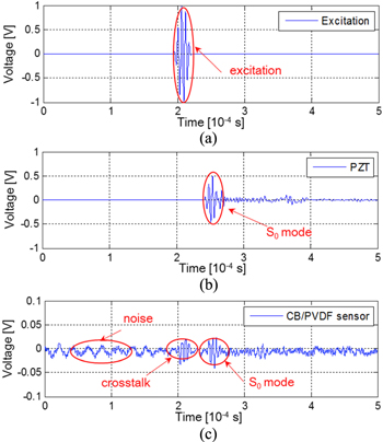
Figure 10. (a) The excitation signal (at 175 kHz); raw GUW signals captured by (b) PZT wafer (PZT2), and (c) CB/PVDF nanocomposite sensor (sensor ①).
Download figure:
Standard image High-resolution image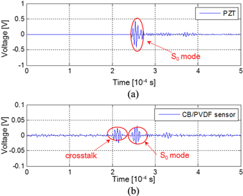
Figure 11. The noise-filtered signals shown in figure 10 by (a) PZT wafer (PZT2), and (b) CB/PVDF nanocomposite sensor (sensor ①).
Download figure:
Standard image High-resolution image
In addition, all the nanocomposite sensors in the sensor network show high consistence in performance in the discussed frequency range (50 ∼ 400 kHz), implying the independence of piezoresistive behavior evidenced by the sensor at the frequency of dynamic elastic disturbance.
4. Further development
With their respective merits and demerits, a variety of sensors are readily available for damage detection and SHM (e.g., PZT, fiber Bragg grating, and macrofibre composites). In terms of practical implementation, a number of spatially distributed sensors are often networked to configure a sensor network. By 'communicating' with one another, the networked sensors holistically and collectively perceive changes in ambient and host structures, meanwhile warranting the desired redundancy of data acquisition. During sensor network configuration, a paramount target is to compromise the 'sensing cost' with 'sensing effectiveness'—to acquire the most information with the fewest sensors. Owing to its distributed nature, a sensor network comprising a limited number of distributed sensors (such as PZT) is likely to 'overlook' information, more or less creating 'blind zones', and deliver inaccurate or even erroneous results.
Light-weight and small, the nanocomposite sensor developed in this study can be coated onto a structure and deployed in large quantities to form a dense sensor network so as to address the concept of a 'quasi-dispersed sensing network' and allow the acquisition of rich information that would be very difficult to achieve using a conventional sensor network with sparsely distributed sensors (e.g., PZT). Diverse sensor networks can be configured conveniently and quickly by flexibly coating a certain number of each. This flexibility is not restricted by the material (metals or composites) or geometric (flat or curved) traits of the host structure to be coated. Advanced processing and molding methods including screen printing, casting and other deposition methods, are currently under the investigation of the authors, showing promise in the implementation of a 'quasi-dispersed sensing network', to be reported in the near future. Featuring these merits, the developed nanocomposite sensor has the potential to achieve a desirable balance between 'sensing cost' and 'sensing effectiveness'.
5. Concluding remarks
A lightweight nanocomposite sensor made of a hybrid of CB/PVDF has been developed to fulfill the in situ acquisition of dynamic elastic disturbance from low-frequency vibration to high-frequency ultrasonic waves. This is the first time that a nanocomposite sensor responsive to dynamic disturbance up to 400 kHz has been documented. Via rigorous material characterization including electrical, morphological and static/dynamic electromechanical response interrogation, the nanoscalar architecture of the sensor was optimized to reach the desired percolation threshold of the CB conductive network (∼6.5 wt%). This has been demonstrated to be sensitive to dynamic elastic disturbance in an ultrasonic regime up to ∼400 kHz with a magnitude as low as on the order of micrometers. The sensor also presents frequency-independent piezoresistive behavior. This study has also revealed that the tunneling effect among nanofillers dominates the sensing mechanism of the sensor in perceiving dynamic particulate motion when a CB nanofiller is in close proximity, but not in direct contact, with the others. In conjunction with a dedicated signal amplification apparatus, the feasibility, correctness and sensitivity of the sensor was examined against conventional metal-foil strain gauge sensors and piezoelectric transducers to demonstrate excellent coincidence between the two types of sensors. Additionally, the sensor shows a much larger gauge factor than conventional strain gauges, therefore demonstrating enhanced sensitivity to weak dynamic signals. Coatable to a structure and deployable in a large quantity, this new type of nanocomposite sensor has blazed a trail for implementing in situ sensing for vibration- or ultrasonic-wave-based damage detection and SHM by striking a compromise between 'sensing cost' and 'sensing effectiveness', while avoiding the shortcomings associated with the use of distributed sensors (e.g., PZT), for instance the insufficient acquisition of information, and the adverse effects of bondlines.
Acknowledgments
This project is supported by the Hong Kong Research Grants Council via General Research Fund (no. 15214414), and by the Hong Kong Innovation and Technology Commission via an Innovation and Technology Fund (ITF) (no. ITS/058/14).