Abstract
The challenges and benefits of microwave-induced microdischarges are reviewed. Transmission lines, resonators and surface wave launchers may be used for coupling microwave power to very small plasmas. Fortunately, microplasmas are typically much smaller than the wavelength of microwaves, and the electromagnetic problem may be treated electrostatically within the plasma. It is possible to trap electrons within small discharge gaps if the amplitude of electron oscillation is smaller than the plasma size. Typically occurring above 0.3 GHz, this condition results in lower breakdown fields than are required by direct current or radio frequency systems. Trapping of electrons also decreases the electrode potential to only tens of volts and makes the plasma density invariant in time. The steady-state microplasma produces electron densities of up to 1015 cm−3 in argon but the electrons are not in equilibrium with the low gas temperatures (500–1000 K). Microwave discharges are compared with other forms of microplasma and guidelines for device selection are recommended. Scale-up of microplasmas using array concepts are presented followed by some exciting new applications.
Export citation and abstract BibTeX RIS

Content from this work may be used under the terms of the Creative Commons Attribution 3.0 licence. Any further distribution of this work must maintain attribution to the author(s) and the title of the work, journal citation and DOI.
1. Introduction
For more than a decade, there has been a growing interest in plasma physics within very small gas discharges. The field of microplasmas includes a highly diverse assortment of plasma devices, each offering interesting and novel plasma science. Perhaps because of this plethora of plasmas, there is no readily accepted formal definition of a microplasma. The broad definition of a plasma with a least one dimension that is less than a millimeter, however, casts a broad net and includes dimensions that are most easily reported in micrometers.
Microplasmas are often dimensionally scaled glow discharge plasmas. The product of gas pressure (p) and discharge characteristic length (d) may be held constant to achieve plasmas with sub-millimeter lengths that operate at atmospheric pressure. One characteristic that is common to almost all microplasmas and glow discharges is that the electrons are not in equilibrium with the heavy particles (ions and atoms). This means that while the electrons are sufficiently energetic to sustain ionization processes (Te > 1 eV), the gas temperature is typically less than 0.1 eV (<1000 K). The non-equilibrium nature of the microplasma sets it apart from arcs for which the electron gas and neutral gas are nearly equilibrated.
While the concept of pd = constant is a useful starting point for understanding a microplasma, there are several aspect of plasma physics that do not scale in this manner. The probability of three-body collisions in low pressure discharges is very small and may be safely ignored in most circumstances. As the plasma size is reduced, however, the coincident increase in gas pressure results in increasingly complex collision reactions including the formation of dimers in noble gases and three-body recombination. These new pathways lead to challenging problems and opportunities. For example, the microplasma pixels in plasma displays rely on efficient excimer formation for the production of UV light. There are several excellent reviews of microplasmas that address the new physics presented by small, high pressure gas discharges that primarily focus on direct current (dc), alternating current (ac), and pulsed input energy sources [1–4].
Frequency is another physical scaling parameter that is influenced by pd scaling. If one considers an electron drifting in an oscillating electric field, it is clear that the electron may traverse the entire plasma dimension (d) prior to the field's reversal if the field frequency is sufficiently low. As one shrinks the plasma dimension to less than 1 mm, it is more likely that electrons in the plasma will be swept to the boundary and lost unless the frequency of the electric field is simultaneously increased to compensate for the reduction in dimensions. At high pressures, electron–neutral collisions reduce the electron mobility and the probability of drift-induced loss. Even so, electrons are not confined by the oscillating field in an atmospheric pressure microplasma until that field frequency is in the microwave band (>300 MHz).
Constructing plasma devices to operate in the microwave domain requires some additional care compared to low frequency systems. This is because the wave nature of the voltage signal must not be ignored. Microwave energy must generally be guided in coaxial cables, waveguides, or microstrip transmission lines. Coupling energy to a plasma requires that the entire electrical system be impedance matched so that electromagnetic waves are not merely reflected from the plasma and absorbed elsewhere. On the positive side, the advent of mobile communication systems has driven the development of low cost microwave electronics. As commodities in mobile telephones, these circuits now produce several watts of microwave power and cost on the order of a few dollars (USD). For many applications and fundamental plasma studies, there are benefits within microplasma physics that justify the added design challenges of microwave circuits, given the low cost of the power sources. This paper focuses on microwave-driven microplasma generation and physics in an attempt to show the particular benefits of such discharges.
2. A brief historical background
Low frequency plasma generation was extensively studied before the advent of microwave plasmas; high-frequency power sources were not technologically feasible in the early years of plasma physics. The magnetron tube is the workhorse of microwave generation, but the concept was not developed until 1921 [5]. These early devices did not operate in the microwave band and had inadequate output power for plasma generation. During the Second World War, the push to develop radar systems brought the magnetron to maturity with microwave output powers in the hundreds of watts. It is easy to imagine that unwanted microwave-induced breakdown within early radar systems represents the first microwave plasma! In fact, the work of MacDonald and Brown [6, 7] at MIT in the late 1940s is recognized as among the earliest to intentionally engineer microwave systems to generate plasma with the specific goal of understanding microwave breakdown. Interestingly, some of the discharge devices studied by MacDonald and Brown were 3 GHz cylindrical resonator cavities with heights as small as 1.6 mm. It is only a slight stretch to credit these two pioneers with the first microwave microplasma.
A problem for radar and communication systems is that microwave electric fields may induce gas breakdown more readily than low frequency and dc fields [8]. For those wishing to create a microplasma, however, this problem is fortuitous and leads to lower starting and operating voltage requirements for the plasma electrodes. The problem of microwave and millimeter wave breakdown also persists in modern systems. As the dimensions of electronics and microelectromechanical systems (MEMS) shrink, and both the frequency and power increase, parasitic breakdown in these systems continues to be studied [8].
In the 1960s microwave plasmas were investigated as harmonic generators, mixers, and amplifiers in an effort to produce higher frequency power signals than was possible using the burgeoning field of electronics [9, 10]. As is now clear, electronics eventually proved more practical. The advancement of microwave plasma technology through the 1970s gave rise to systems for gas phase processing [11], plasmas with a physical extent longer than the electromagnetic wavelength [12], and low pressure systems that used electron cyclotron resonance [13]. The circle was completed as these advancements in plasma physics were incorporated into plasma processing systems that were critical to the evolution of highly integrated, high-frequency electronics [14].
Returning to the domain of microplasmas, miniaturized plasma generators operating at 450 MHz were described in the late 1990s. These devices were scaled-down inductively coupled plasmas with dimension of several millimeters and only operated below approximately 10 Torr [15]. The first true microwave microplasma device operating at 1 atm was described by the Broekaert group in 2000. The device leveraged microstrip transmission line concepts to form an argon plasma in a glass channel located between a narrow microstrip resonator and a ground plane [16]. The reactor consumed 40 W of power at 2.4 GHz, but subsequent design modifications resulted in a fully functional microplasma source operating at low power that was suitable for chemical analysis applications [17]. At approximately the same time Kono's group produced an atmospheric pressure microplasma using traditional waveguides that operated at 2.45 GHz and approximately 100 W [18]. In the remainder of this paper, we shall examine the various configurations of microplasma generators and describe some of the fundamental properties of these discharges as compared to low frequency microplasmas. In addition, the scaling of arrays of individual microplasmas toward larger areas and volumes will lead to a brief synopsis of applications.
3. Microwave-driven microplasma topologies
Before discussing microplasma characteristics, it is first necessary to understand the basic topologies currently used for coupling microwave energy to a discharge. As previously mentioned, microwaves must be guided in specialized structures (e.g. waveguides, coaxial lines, microstrip lines). The details of these structures are of secondary importance because each possesses a characteristic impedance (Z0) which describes the ratio of E/H (or V/I) for a wave propagating in the guide. Following the principle of maximum power transfer, energy is transferred from the power source to the waveguide when the output impedance of the source is matched to the transmission line
 . The asterisk denotes the complex conjugate, but most systems have standardized on Z0 = 50 Ω and avoid complex reactances. The same impedance condition is true for the transition from the transmission line to the plasma
 . The design of the microwave circuit entails creating structures that approximately follow these rules in order to avoid the reflection of waves from interfaces and the subsequent reduction in energy transfer from the power source to the plasma. (Microwave reflection due to an impedance mismatch is analogous to the reflection of light from a dielectric interface of differing refractive indices.) The plasma impedance Zp is typically composed of a resistive component due to electron collisions, a capacitive component due to plasma sheathes (and free space) and an inductive component due to electron inertia. This model also applies to microplasmas, but the inductive component is usually small except at low gas pressure or high frequency [19]. The electrical impedance model of the microplasma will depend on the discharge conditions and therefore some degree of tuning of the external circuit is needed. In addition, the conditions for plasma ignition require a high electric field strength when there is no plasma such that Zp → ∞.
Three basic topologies are sketched in figure 1. For illustrative purposes, the transmission line is a microstrip which consists of a thin metal line (∼1 mm in width) separated from a large ground plane by a layer of low-loss dielectric. Other structures such as coaxial cables and waveguides may be substituted with the same general result, however. The simplest structure is the transmission line device of figure 1(a) [20]. Microwave power enters the Z0 = 50 Ω microstrip from the left and the electric field between the end of the transmission line and the ground pad sustains the plasma. In this configuration maximum power transfer to the plasma occurs if Zp = 50 Ω. For a typical discharge gap shown, this requires an electron density of ne ∼ 1015 cm−3 at 1 atm (Ar). Any impedance mismatch will cause the incoming wave to reflect back to the power source and be lost. Sometimes tuning elements are added to the transmission line to reduce reflected losses. A more complete discussion will follow, but next we will discuss the resonator system illustrated in figure 1(b). Although superficially similar to the simple transmission line, the resonator consists of a microstrip that is terminated on the left side by a short-circuit (via) to ground. The opposite end of the microstrip is an open circuit. Microwaves introduced at a specific location on the resonator will reflect from both the short and open circuits. If the frequency is chosen such that these reflections constructively interfere (e.g. 1/4 of the wavelength is the length of the strip), then a standing wave forms on the resonator and an intense electric field is present between the open end and the ground pad. Any reflected wave from the plasma discontinuity is primarily recycled by reflection from the grounded end of the microstrip line. A quarter-wave resonator is illustrated, but half-wave [21–23] and 3/4-wave resonators [24, 25] behave in a similar fashion. A third microwave coupling strategy is sketched in figure 1(c). Either a transmission line or a resonator structure may be used to induce an electric field in the discharge region. A dielectric tube is inserted in the high field location. Once breakdown occurs, a surface wave can be launched from the microstrip line and propagate along the plasma/tube interface. There are several examples of micro surface-wave devices in the literature [26–29]. These capillary-type microplasmas may extend more than 10 cm in length and are interesting for coating the inside of capillaries, as complex UV/VUV optical systems, or for delivering plasma species to locations tens of centimeters distant from the microwave circuit. This review focuses on microstrip-based implementations of the first two topologies; readers interested in surface wave propagation are referred to the referenced papers.

Figure 1. Three topologies used to couple microwave power to a microplasma: (a) a simple transmission line, (b) a microwave resonator and (c) a surface wave device.
Download figure:
Standard image High-resolution imageThe transmission line structure of figure 1(a) is repeated in the form of a circuit schematic in figure 2(a). If the characteristic impedance of the transmission line is 50 Ω, then a perfectly matched traveling wave will have a voltage amplitude given by P = V2/2Z0, where P is the input power. For an input power of 1 W, the voltage amplitude is 10 V. When no plasma is present, however, the wave reflects from the open circuit at the discharge gap and the resulting standing wave has a maximum amplitude of 20 V as shown in the sketch. (The location of this maximum depends on the length of the T-line and can be controlled with a movable short [27].) At atmospheric pressure, this voltage is insufficient to breakdown all common gases and the transmission line microplasma must use either an external ignition source or a very large input power must be supplied (P ∼ 100 W). Once ignited, power is coupled to the plasma with high efficacy only if Zp is near Z0 and the reactance of the plasma is small. A simple calculation for Zp = Z0 = 50 Ω shows that the microplasma density should be the order of 1015 cm−3 to maximize absorbed power; this is confirmed by experimental measurements [18, 30]. The dashed line in figure 2(a) shows the voltage in the case of a well-matched plasma impedance (P = 1 W) which now has a much smaller standing wave pattern. The plasma density is quite high and frequent electron–neutral collisions cause the gas temperature to reach over 2000 K [31, 32]. The microplasma, however, is not in equilibrium and is distinct from an arc. Because power is coupled to the plasma only for Zp ∼ 50 Ω, any glow-to-arc transition is avoided because the lower impedance of the arc will also reflect microwave power [33]. This stabilization mechanism plays a role which is similar to that of a ballast resistor in dc plasmas. The self-pulsing instability of the dc microplasma caused by parasitic capacitance is avoided, however [34].
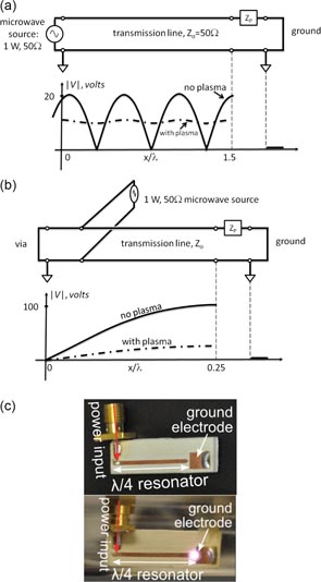
Figure 2. Transmission line equivalent circuits and voltage distributions for (a) a 50 Ω transmission line and a microplasma impedance Zp, (b) a quarter-wave transmission line resonator. The solid line represents a typical voltage distribution with no plasma present. The dashed line shows the approximate voltage waveform with a typical plasma impedance for an input power of 1 W. Photographs of a 1 GHz quarter-wave (λ/4) resonator in (c) illustrate a 20 mm long microstrip device with (bottom) and without (top) a microplasma.
Download figure:
Standard image High-resolution imageThe schematic of figure 2(b) will aid in showing the differences between a resonator and a transmission line microplasma. The input impedance along the length of the resonator varies between 0 Ω at the via on the left and infinity at the open-circuit discharge gap. Power is applied at an intermediate position where the impedance is 50 Ω. Most systems are designed such that the input position is chosen with no plasma present and maximum power is transferred to the resonator prior to plasma ignition. Specific design equations can be found in [35]. The resonator typically has a quality factor Q greater than 100, and the microwaves reflect between the via and the gap on the order of Q times. At resonance, each reflection increases the discharge gap voltage. The sketch of figure 2(b) provides a representative case of the quarter-wave resonator shown in figure 2(c) which is made from copper on a RT/Duroid substrate for which electromagnetic simulations [30] show that 1 W of input power results in sinusoidal standing 1/4-wave with a magnitude of 100 V at the gap. A comparable half-wave resonator in the form of a split-ring would produce twice this voltage and would be sufficient to breakdown atmospheric pressure argon in a 100 µm discharge gap [30]. With a discharge present in the gap, the plasma impedance absorbs a fraction of the power from each reflection along the resonator. A perfect impedance match is unnecessary because the multiple reflections allow for O(Q) opportunities for the plasma to absorb power. The presence of the plasma impedance has two important effects on the resonator system. First, the absorption of energy by the plasma's resistance Rp reduces the Q and decreases the gap voltage as shown by the dashed curve in figure 2(b). Measurements and simulations show that the peak-to-peak voltage is reduced to approximately 30 V in the presence of an argon plasma at 1 atm [30]. The second effect is more subtle: the plasma reactance, primarily due to the capacitive plasma sheaths at high pressure, shifts the resonance frequency of the device downward [38]. The combination of plasma resistance and reactance shift the input impedance away from 50 Ω and reflection of the input power increases. The device in figure 2(c) typically operates with 20–50% reflected power. Power coupling is found to be most efficient to a plasma with Rp ∼ 1 kΩ which corresponds to a typical electron density of 1014 cm−3 in atmospheric pressure argon [30, 33]. If the plasma were to become unstable and transition to an arc, the resulting low plasma resistance would essentially short-circuit the resonator and almost all microwave power would be reflected. In this manner, the resonator system stabilizes the microplasma against the glow-to-arc transition. Input powers of up to 40 W have been applied to single microplasmas and the resonator circuit successfully prevents arcing [33].
In this section, coupling microwave power to a plasma through a transmission line and through a resonator have been discussed. Each device prevents that glow-to-arc transition by reflecting microwave power should the plasma resistance suddenly drop to that of an arc. The transmission line, however, couples power most efficiently to a low impedance, high density plasma which is beginning to approach thermal equilibrium in atmospheric pressure argon. The resonator microplasma will self-start, but impedance mismatching occurs even for a relatively resistive plasma. This limits the electron density of the resonator device to an order less than the transmission line device and also results in lower gas temperatures.
4. Microplasma structure
Although the external microwave circuit ultimately determines the plasma character, the internal structure of the microplasma is similar for both transmission line and resonator devices. Figure 3 shows a close-up view of the discharge gap region. The electromagnetic nature of the microstrip may be replaced by a simple voltage source because the microplasma size is much smaller than the wavelength. High-frequency magnetic fields can also be ignored and the microplasma essentially experiences the quasi-static electric field that is imposed on the discharge gap. One may now observe that the microplasma is quite similar to a frequency- and dimensionally-scaled capacitively coupled plasma.

Figure 3. Close-up sketch of the microplasma region in figure 1. Ions are immobile in the microwave field, but electron oscillation amplitude is a critical parameter. For short microplasmas (d ≪ λ), the transmission line model reduces to the quasi-static case of a voltage applied to a microelectrode as shown.
Download figure:
Standard image High-resolution imageFirst we consider breakdown in the microgap due to a small number of 'seed' charges. At low frequency, both the ions and the electrons oscillate in the electric field and will transit the discharge gap where they are lost to the electrodes. This is also the case for dc plasmas and so a large breakdown potential must be applied to ensure that seed electrons have a high probability of ionizating collisions before being lost. At microwave frequency, however, the ions remain immobile as drawn in figure 3. The electrons, however, will oscillate in response to the applied voltage. There are two cases which are important. (1) The electron amplitude of oscillation is larger than the discharge gap size (d) and the electrons are substantially lost to the electrodes. (2) The electron amplitude of oscillation is less than d and the electrons are efficiently trapped in the discharge gap. At atmospheric pressure, the electron collision frequency is the order of 3 × 10¹² Hz and is always much greater than the electric field frequency. With this constraint one finds that the relationship between gap voltage (Vrms), gap size (d), and oscillation frequency is given by [8]

where m is the electron mass and νc is the electron–neutral collision frequency. Above the critical frequency fcr the electrons are mostly confined in the discharge gap and the breakdown field is as much as three times lower than the low frequency or dc field [8, 36]. For a typical microplasma with d = 100 µm the frequency should be greater than 250 MHz to avoid excessive electron losses during breakdown in atmospheric pressure argon (assuming an electrode voltage of Vrms = 140 V prior to plasma ignition).
Electron confinement in high-frequency fields not only aids in gas breakdown, but it also reduces electron drift to the electrodes during operation. All else being equal, the reduction of electron losses creates a higher density plasma that neither extinguishes nor varies substantially during each cycle. A fluid model for a 500 µm gap discharge in helium at 1 atm nicely illustrates the evolving plasma character with frequency [37]. Using a conventional radio frequency (RF) plasma frequency (10 MHz), the microdischarge is found to operate in the γ-mode with ionization being driven by secondary electrons from the electrodes. Ion generation is found to occur primarily within the sheath regions. The electrode voltage during plasma operation is 190 V and the central plasma appears to oscillate between the two electrodes and nearly extinguishes twice each cycle. At a drive frequency of 50 MHz, the discharge transitions to the α-mode and the bulk plasma electrons are heated by the rf electric field. This frequency is in the vicinity of fcr for d = 500 µm and the bulk plasma electrons exhibit minor oscillation between the electrodes. At 1000 MHz, however, the electrons are well-confined within the discharge gap and the central plasma density is nearly constant. In addition, the modeled electrode voltage during plasma operation decreases to only 40 V at 1 GHz. Experiments performed between 0.45–1.8 GHz confirm these conclusions [38].
To examine the internal structure of the microwave microplasma, including the sheath dynamics, we present a particle-in-cell Monte Carlo (PIC-MC) simulation for a f = 10 GHz discharge sustained within a 1D gap with d = 100 µm in atmospheric pressure argon (figure 4). Readers are directed to [39] for a comprehensive fluid model that includes a rich set of reactions; in this PIC-MC simulation we focus on the time-domain plasma sheath potential. The simulation uses XPDP1, a 1D-3V PIC code with conducting planar boundary electrodes [40]. Anticipating the experimental electron density of 1014 cm−3, we find the Debye length to be λD = 1.3 µm and then divide the simulation domain into 200 cells with Δx = 0.7 µm such that

The electron plasma frequency should be approximately ωp = 6 × 10¹¹ rad s-1, so the simulation time step was chosen to be Δt = 3 × 10⁻¹³ s such that

The 200 cells were populated with 60 000 macro-particles, giving 300 per computational cell and 772 particles per Debye length. The free-space wavelength of the 10 GHz input energy is 30 mm (≫d), therefore the quasi-static approximation is valid and a sinusoidal voltage is applied to the left electrode while the right electrode is grounded, V(t) = Vpk cos(2πft). The PIC simulation does not attempt to resolve the gas temperature, so we have used experimental data and set Tgas = 600 K. Only electron–neutral collisions, single-step excitation, and single-step ionization were included. Three-body reactions affect plasma behavior [41] but have not been included at this time.
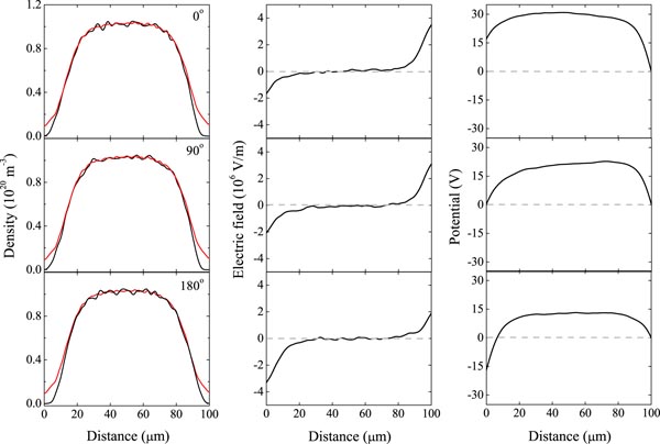
Figure 4. Simulated electron and ion density (red line), microwave electric field and potential in a 10 GHz microplasma in 1 atm of argon (d = 100 µm). The 10 GHz voltage (17 V) is applied to the left planar electrode and the right electrode is grounded (see figure 3) in this 1D model. Plasma sheath regions exist for 0 < x < 10 µm and 90 < x < 100 µm and depend on the applied voltage.
Download figure:
Standard image High-resolution imageFigure 4 plots the electron density, self-consistent electric field, and plasma potential as a function of distance within the d = 100 µm plasma. Three snapshots in time are provided (ωt = 0°, 90° and 180°) for an applied voltage of V(t) = 17 cosωt V at the left electrode (x = 0). The central plasma density is found to be nearly static in time and space between 20 and 80 µm with a uniform quasi-neutral density of 1020 m−3 in agreement with Stark broadening measurements. At ωt = 0o one observes a sheath with a potential of 25 V near the ground electrode (right side) that extends 10 µm into the plasma. The peak electric field is 3 × 10⁶ V m−1 at the wall, but the dense central plasma volume shields the potential and allows a bulk electric field ≪106 V m−1. The electron density is depleted in the right sheath region, but the ion density is immobile at 10 GHz and does not vary in time. At the powered electrode (left side), the potential is +17 V. Here the sheath is partially collapsed and there is a non-zero electron density that makes contact with and is lost to the powered electrode.
The instantaneous electrode potential is zero for ωt = 90o in the second row of plots in figure 4. Both sheath regions exist but the discharge is not entirely symmetrical. This is because the electrons are not responding instantaneously to the 10 GHz electric field due to electron inertia. This results in a small plasma inductance [19] because ω is no longer negligible compared to the electron collision frequency, even at gas pressures of 1 atm.
The final set of simulation results show the plasma at ωt = 180o. The data of figure 4 indicate that the right-side sheath has collapsed and some electron flux is reaching the ground electrode. Ions remain stationary in the 10 GHz field. There will be, however, a constant ion flux due to highly collisional drift in the time average plasma potential revealed in figure 4. Ions in the sheath region will experience an average sheath potential of 10–15 V. This would be sufficient to accelerate the ions to an energy near the sputtering threshold of metal electrodes, but the ion mean free path is <0.1 µm (depending on gas type and temperature). The collisions within the 10 µm sheath suppress the average ion energy at the electrodes to be less than 1 eV which eliminates electrode sputtering and plasma source lifetime problems. Lifetime testing is discussed in the following section.
5. Lifetime testing
Both simulations and measurements of the electrode voltage that is required to sustain a microwave microplasma suggest that ion energies should be below the sputtering threshold. For this reason, high-frequency microplasmas are often operated in direct contact with the electrodes, although dielectric coatings may be used in chemically reactive gases or low pressures [19]. In 2005 we operated a half-wave split-ring resonator fabricated on Al2O3 with gold electrodes for 50 h in atmospheric pressure air without damage [42]. In fact this same device is still being used in 2014. In this work we now present a more controlled experiment to determine device lifetime.
The test device consisted of an array of five individual quarter-wave resonators (see figure 2(c)) operated in parallel from a single 0.4 W power source at 1 GHz. As shown in figure 5, each resonator was 20 mm long and 1 mm wide and was fabricated from copper on a substrate of RT/Duroid polymer. The discharge gap was d = 100 µm. The high voltage ends of the five resonators were covered by a ceramic limiter in order to confine the plasma to the distal 0.3 mm of the resonator. The array was placed in a stainless steel chamber which was backfilled with argon to 1 atm. Because there was no gas flow during testing, the argon would slowly become contaminated by water vapor and hydrocarbons from the RT/Duroid substrate. Therefore, once per week the argon was flushed and replaced.
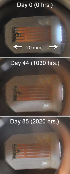
Figure 5. Lifetime testing of a five-element array of λ/4 microstrip resonators shows operation for more than 2000 h (P = 0.4 W, 1 atm argon). Changes in the plasma color are due to contamination of the argon gas.
Download figure:
Standard image High-resolution imageFigure 5 shows the microplasma after t = 0, 1030 and 2020 h of operation; the change in discharge color was due to the aforementioned argon contamination. At the end of the lifetime experiment (2020 h), the device was sacrificed by removing the ceramic limiter and microscopically viewing the discharge gap. As shown in figure 6, the copper electrodes are coated with a thin film of contamination that is believed to be carbon from the adhesive that attaches the copper microstrip to the RT/Duroid substrate. The discharge gap dimensions, however, are observed to be unchanged and there is no rounding or beveling of the copper surfaces due to sputtering. Although the experiment was halted to make the observation, the device could reasonably be expected to operate far beyond 2000 h. It should also be noted that while this laboratory device was fabricated from uncoated copper electrodes and polymer, and production-worthy construction consisting of refractory metals and ceramics would be expected to operate even longer.
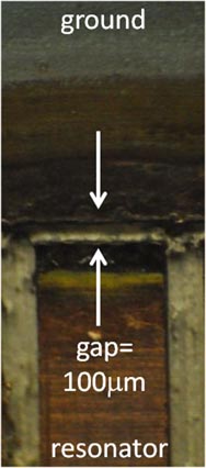
Figure 6. The 1 mm wide copper microstrip electrode and ground plane show no erosion or beveling of the 100 µm discharge gap due to sputtering after 2000 h of operation in argon. Dark deposits are believed to be from carbon that outgases from the polymer substrate.
Download figure:
Standard image High-resolution image6. Plasma characteristics
In this section the constituent properties of microwave microplasmas are discussed. Electron density, rotational temperature [43], and metastable density are spatially mapped within a single microplasma operating in 1 atm of argon within the controlled environment of a sealed chamber. Figure 7 shows the spatially and spectrally resolved intensity due to Hβ emission from an argon microplasma (+500 ppm H2) sustained by a quarter-wave microstrip resonator similar to figure 2(c). The tip of the 1 mm wide resonator is outlined by a dashed white line on the left. The tapered ground electrode is indicated on the right. The 100 µm discharge gap is located at x = 1.4 mm. The upper frames show that the discharge formed two filaments of approximately 0.2 mm width for a 1 GHz input power of 0.35 W. As the power increased to 0.62 W (lower frames), the two regions merged into a single, more intense microplasma. This filamentation is unique to argon gas and has not been observed in other gases. The microplasmas initially form in the discharge gap region, but in the absence of any containment structures the steady-state plasma extends beyond the 100 µm discharge gap to the right and left by approximately 1 mm.
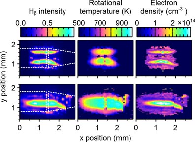
Figure 7. Spatially resolved optical diagnostics of a 1 GHz quarter-wave resonator microplasma operating at 0.35 W (top) and 0.62 W (bottom) at 1 atm. Optical emission from hydrogen atoms (Hβ, 486.1 nm) on the left shows that the argon microplasma extends outside the discharge gap and across the microstrip electrodes (outlined in white). The rotational temperature is determined from the molecular emission spectrum of CH (middle). Stark broadening of the Hβ emission indicates that the peak electron density is 3 × 1014 cm−3 (right). Reproduced from [43].
Download figure:
Standard image High-resolution imageThe 2D spatially resolved rotational temperature is extracted from the measured emission spectra of the CH molecular fragment from 425 nm < λ < 437 nm (trace hydrocarbons in the discharge are from the polymer substrate as discussed above). Synthetic spectra are then fit to the CH emission to determine the rotational temperature. Assuming that the rotational temperature is in equilibrium with the translational gas temperature, we observe that the temperature profiles are somewhat wider than the emission profiles and range between 700–800 K (figure 7) at these power levels. Finally, the spectral line-width of the Hβ line at 486.1 nm is deconvolved from instrument and collisional broadening using the CH rotational temperature. The remaining Stark broadening indicates that the electron density profile matches the Hβ emission profile and peaks at 3 × 1014 cm−3. It may be noted that the Hβ intensity represents a line integration of emission from the discharge and therefore the reported electron density represents a weighted average along this line of sight. Abel inversion of the spatially resolved Stark broadening suggests peak electron densities in the central region approximately a factor of 2 greater, and reaching 1015 cm−3 at higher power levels of 1.5 W if the microplasma is assumed to be cylindrically symmetric. These 3D effects are not captured by the 1D PIC simulations above but are in agreement with other fluid simulations [38, 44].
The argon metastable density is determined from the absorption of 801.4 nm photons from a diode laser which is wavelength scanned as it passes through the microplasma. The laser pumps the 1s5–2p8 transition of argon and the absorption depth provides the density of the 1s5 argon metastable state. The laser was focused to a 30 µm diameter beam which could be mechanically scanned through the y-direction of the microplasma within the discharge gap (see figure 7) providing spatially resolved line-integrated metastable density. By assuming that the discharge is cylindrically symmetric along the axis of the microstrip, the density profiles may be Abel inverted to provide the radially resolved argon metastable density profile of figure 8 [45]. For a plasma power less than 200 mW, the argon metastable density is centrally peaked, similar to the temperature and electron density profiles of figure 7. At higher powers, however, we observe that the central core of the microplasma becomes depleted of metastable argon as shown in figure 8 (P = 1.2 W, d = 500 µm). The maximum metastable density saturates at (0.8–1) × 1013 cm−3 for any input power greater than 500 mW, but the annular volume of this peak metastable concentration expands radially outward with increasing power.
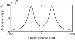
Figure 8. The radial distribution of Ar(1s5) metastable atoms in a microplasma operating at 0.9 GHz in atmospheric argon (d = 500 µm) as measured by spatially resolved diode laser absorption after Abel inversion. The peak density occurs in a cylindrical volume approximately 150 µm from the metastable-depleted core of the microplasma. Reproduced with permission from [45]. Copyright 2011, AIP Publishing LLC.
Download figure:
Standard image High-resolution image7. Comparison of microplasmas
The vast variety of microplasma geometries, excitation frequencies and voltages offers many opportunities for both scientific exploration and practical applications. This same diversity, however, makes a fair comparison impossible due to the wide range of discharge geometries, power densities and operating conditions. Nonetheless, a representative sample of microplasma characteristics is presented in table 1. These data provide typical results that were determined through robust diagnostic methods. There was no attempt to report the highest or best data, however. In order to provide some uniformity, the listed data were chosen for atmospheric pressure argon to the extent possible.
Table 1. Representative microplasma characteristics for dc, DBD, RF and microwave frequency devices.
| Microplasma type | Tgas (K) | ne (cm−3) | Te (eV) | Metastable density nm(cm−3) | Discharge voltage (V) |
|---|---|---|---|---|---|
| Dc | 500–1000 [47] | 1014–1015 [48, 49] | 0.9 ± 0.3 [49] | (0.5–1) × 1014 [47] | 220–320 [48, 49] |
| DBD peak | 1000 [50] | >1016 [51] | — | 1013 [50] | 300–800 [51] |
| DBD average | 350 [52, 53] | <1011 [53] | 1.2 [53] | — | 10 000 [53] |
| RF (He/Ar) | 330 [54] | <1011 [55] | 2.5 [55] | 109–1011 [54] | 300 (est) [57] |
| Microwave resonator | 500–800 [26] | 3 × 10¹⁴ [26] | 1.2–1.5 [56] | 1013 | ∼20 [26] |
| Microwave transmission line | 1000–2000 [26] | >1015 [18, 26] | 1.2 (in He) [18] | — | ∼35 [26] |
For dc through microwave operation, the time-averaged electron temperature appears to be approximately 1.2 eV. The exceptions to this general observation are pulsed systems for which the initial electron energy of the plasma can be higher [41]. Gas temperature is highly dependent on power density, but a pattern still emerges. Microplasmas which are continuously sustained and do not have transient ionization behavior (dc and microwave) typically have gas temperatures between 500–2000 K. Dielectric barrier discharges are transient discharges which self-extinguish as plasma charge accumulates on the insulating electrodes. The low duty cycle of the dielectric barrier discharge (DBD), which may be less than 1% for filamentary discharges, reduces the time average rotational temperature to only slightly above ambient. Time-resolved diagnostics in a DBD [50] show that the peak temperature is in line with other sources (∼1000 K). The RF microplasma also has periodic γ-mode heating each cycle and appears to be lower in temperature as well. Electron density is also a strong function of power density, making comparisons difficult. For continuous microplasmas, however, the electron density is typically 1014–1015 cm−3. Inherently low duty cycle microplasmas exhibit lower average electron density (<1011 cm−3), although the electron density readily exceeds 1016 cm−3 for the short, intense discharges found in filamentary-mode discharges.
Operating voltages are also strongly dependent on the discharge gap geometry, materials selection, and gap length in microdischarges. The DBD has a wide variety of operating potentials which are typically kilovolts for millimeter-scale gaps, but the lowest values are attributed to thin dielectrics, reduced pressure, and small gaps. Dc and RF frequencies both allow free plasma electrons to transit the discharge gap and be lost. These devices typically operate around 300 V. In the dc case, the energetic ion flux may lead to erosion of the electrodes and short lifetimes [46]. It is only at microwave frequencies when the critical frequency (fcr) is exceeded that electrode voltages significantly decrease. The microwave discharge may be sustained by several tens of volts because electrons are trapped in the discharge gap by the high-frequency oscillating electric field. In applications where low voltages, long lifetime, high electron density, and steady-state operation are desirable, the microwave discharge should be considered.
8. Scale-up: arrays
The atmospheric microplasma is difficult to dimensionally scale to larger sizes, so the focus has turned to generating arrays of microplasmas. In addition to interesting plasma physics [58], arrays of microplasmas offer broad area light sources [59], parallel processing of large gas flows [60], treatment of surfaces [61], and novel electromagnetic structures [62].
If we are considering hundreds or thousands of microplasmas, it is not practical to provide a microwave source for each plasma. It is almost as difficult to use power splitters to evenly divide a single higher power microwave generator's output. Fortunately, the microwave resonator provides an inherent physical solution to this dilemma. The tendency for sharing energy among identical, high-Q resonators is stronger than our intuition. As an example, a half-wave split-ring resonator (0.45 GHz, Q ∼ 200) is shown in figure 9. The ring-shaped resonator is fabricated on a RT/Duroid dielectric substrate with a continuous ground plane (not visible). It sustains an atmospheric helium microplasma in a 200 µm discharge gap. An identical resonator, also fabricated on a ground plane, is attached to the backside of the first resonator and is visible in the handheld mirror. Microwave power is only supplied to the backside ring resonator. The two back-to-back ground planes separate the two resonators and almost entirely isolate the electromagnetic coupling between the two devices, yet the unpowered resonator (front) also ignites and sustains a microplasma of the same intensity. This demonstrates the fundamental result of coupled mode theory (CMT) [63]: that even weak coupling is sufficient to allow identical, high-Q resonators to evenly share energy.

Figure 9. Energy sharing between two identical split-ring resonators demonstrates CMT. The two microstrip rings resonate at 450 MHz, but only the backside device, visible in the mirror, is connected to a power source. The unpowered front-side device also ignites and sustains an atmospheric pressure helium microplasma (d = 200 µm) even though the two resonators are separated by a continuous ground plane (not visible) such that the electromagnetic coupling is very weak.
Download figure:
Standard image High-resolution imageThe geometry of the split-ring resonator of figure 9 does not lend itself to fabrication in dense arrays. We can, however, apply the principles of CMT to short, quarter-wave microstrip resonators similar to figure 2(c). If we supply energy at the frequency of the first eigenmode of the CMT solution for an array of quarter-wave resonators, it is possible to produce lines [64, 65], circles [66] and surfaces [67] of microplasmas driven by a single microwave power source. It should be noted, however, that this principle does not apply to transmission line style systems with little or no resonance.
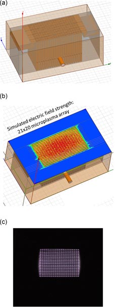
Figure 10(a) shows an example of a 420-element microplasma array that consists of 20 dielectric substrates stacked to form a rectangular volume. Each substrate hosts 21 quarter-wave resonators on its front surface. Only the high-field tip of each resonator is exposed at the top of the resonator block to form a 21 × 20 array of microplasmas measuring 18 mm by 15 mm. Each dielectric substrate also has a copper grounding strip fabricated on its back surface that extends behind the 21 resonator tips and contacts the two opposite faces of the copper-clad rectangular volume. Each embedded grounding strip is offset from its adjacent row of 21 resonators by a 0.13 mm Teflon sheet which sets the discharge gap distance, d = 130 µm. A single power source is attached to the central resonator of each board through a coaxial line extending from the front of the block as shown. At resonance, this power is shared among all of the resonators in the array. An electromagnetic simulation of the structure with a 20 × 21 array of resonators is shown in figure 10(b). The intense regions of electric field are seen to cross the upper surface from each resonator tip to the adjacent grounding strips. Energy and electric field intensity is somewhat uniform, but decreases near the edges of the array where each resonator has fewer nearby neighbors and less coupling. The 20 × 21 array is shown sustaining an array of microplasmas on its top surface in figure 10(c). The 100 Torr argon microplasmas are consuming a total of 10 W of power at 0.59 GHz (25 mW/microplasma). This device was constructed from Teflon and RT/Duroid which limited the maximum power density and temperature on the surface and restricted the power required for full operation at 1 atm. Future devices will be constructed from high temperature materials. Challenges in array scaling include impedance matching of very large arrays to 50 Ω power sources and attaining uniform power sharing over greater distances.
Figure 10. Two dimensional arrays of microwave microplasmas (d = 130 µm) may be operated in parallel from a single microwave power source. (a) A solid model showing a 21 × 20 array of λ/4 resonators embedded in dielectric and surrounded by a copper boundary; the high potential tip of each resonator is exposed on the top surface. (b) A 3D electromagnetic simulation demonstrates the uniformity in the magnitude of the electric field generated between each resonator tip and a series of embedded copper ground strips across an active area of 18 mm by 15 mm. (c) A microplasma array operating in 100 Torr argon (10 W) on the top surface of the device modeled in (b).
Download figure:
Standard image High-resolution image
9. Applications
High-frequency microplasmas are finding utility in several applications. One of the earliest was as an excitation source for gas sensors [68, 69]. The spectrum of light emission from the microplasma is used to determine the atomic and molecular species present in gas samples. The small size and low voltage operation make microplasmas a convenient light source in miniaturized lab-on-a-chip systems. VUV light emission from microwave devices has also been used as a soft ionization source for mass spectrometry [70]. The photon energy can be tuned by selecting the resonance radiation from various noble gases, and large molecules may be photoionized with less fragmenting than caused by conventional e-beam ionizers. A last example of microplasma-based sensors is optogalvanic spectroscopy which employs a half-wave split-ring resonator [71].
Free electrons generated by the microplasma can attach to and charge airborne particles, replacing radioisotopes used in particle counting systems [72]. These charged particles may also be trapped and concentrated inside the potential well created by the microplasma as shown in figure 4. Another recent development is the use of the dense electron gas of the microplasma as a semiconducting medium [73]. The MOPFET (plasma transistor) promises to be more robust than semiconductor devices in high temperature and high radiation environments. Finally, the high metastable density of the microplasma can be used as a lasing medium for diode-pumped lasers. Using a linear array of 15 quarter-wave resonators, a sufficient path length of microplasma was obtained to produce optical gain and lasing [74]. The microplasma laser is an exciting harbinger of many future applications.
10. Conclusion
Microscopic volumes of high density, non-equilibrium plasma may be initiated and sustained using microwave voltages. These voltages may be applied to the plasmas through direct contact with simple metal electrodes. The electrodes are not eroded by sputtering because the microwave voltages needed to sustain the plasma are the order of tens of volts. Collisional transport of ions through the time-average sheath potential reduces the ion energy to the order of 1 eV at the electrode. Because the ion energy is low, copper electrodes show no erosion after 2000 h of argon microplasma operation at 1 atm.
Resonator structures produce sufficiently high voltage to self-ignite microplasmas, even at pressures of 1 atm. The microplasma loads the resonator in a manner that causes power reflection in the event that the plasma attempts to transition from a non-equilibrium plasma to an arc. The plasma loading of the resonator also limits the minimum attainable plasma resistance and restricts electron density to less than 1015 cm−3. Transmission lines, on the other hand, couple power to lower plasma resistances. The structures sustain higher plasma densities as a result of optimal power absorption near Rp = 50 Ω. Both transmission lines and resonators 'ballast' the plasma by reflecting additional microwave power as the plasma density increases.
Microwave and dc microplasmas are both continuous discharges with similar plasma characteristics including electron density (<1015 cm−3), electron temperature (1 eV), metastable density (1013 cm−3), and gas temperature (500–1000 K). The sustaining voltage, however, is an order of magnitude lower for microwave plasmas. PIC simulations help visualize the microplasma and confirm the low electrode voltages. In contrast, dielectric barrier discharges and radio frequency microplasmas exhibit transient ionization. While their peak plasma densities may be high, the time-average properties are less intense by orders of magnitude. Lower frequency electric fields (< fcr) do not trap electrons in the discharge gap which increases electron drift losses to the electrodes and also the required breakdown field.
The natural tendency of identical high-Q resonators to share energy can be leveraged to generate stable arrays of microplasmas from a single microwave energy source. Arrays of microplasmas offer many interesting new applications including thin film deposition, plasma-based metamaterials and microplasma lasers. Microplasmas physics, technology and applications are still in an early stage of development and there are many scientific and engineering challenges ahead.
Acknowledgments
This work was supported by the DARPA Microscale Plasma Devices program (Dr Dan Purdy, Program Manager) under awards FA9550-12-1-0006, managed by Dr John Luginsland through AFOSR, and N00014-13-1-0619 managed by Stephen Pappert through ONR.