
Abstract
This study reports a novel approach to the implementation of 3D carbon nanotube (CNT) interdigitated finger electrodes on flexible polymer, and the detection of strain, bending curvature, tactile force and proximity distance are demonstrated. The merits of the presented CNT-based flexible sensor are as follows: (1) the silicon substrate is patterned to enable the formation of 3D vertically aligned CNTs on the substrate surface; (2) polymer molding on the silicon substrate with 3D CNTs is further employed to transfer the 3D CNTs to the flexible polymer substrate; (3) the CNT–polymer composite (∼70 μm in height) is employed to form interdigitated finger electrodes to increase the sensing area and initial capacitance; (4) other structures such as electrical routings, resistors and mechanical supporters are also available using the CNT–polymer composite. The preliminary fabrication results demonstrate a flexible capacitive sensor with 50 μm high CNT interdigitated electrodes on a poly-dimethylsiloxane substrate. The tests show that the typical capacitance change is several dozens of fF and the gauge factor is in the range of 3.44–4.88 for strain and bending curvature measurement; the sensitivity of the tactile sensor is 1.11% N−1; a proximity distance near 2 mm away from the sensor can be detected.
Export citation and abstract BibTeX RIS
1. Introduction
Flexible sensors have been extensively investigated recently for incorporation into clothing or for direct attachment to the body of a human/robot for wearable smart devices [1] and humanoid robot system [2] applications. Flexible sensors can also be adopted as artificial skins, which mainly serve as sensing interfaces to realize information exchange and to avoid damage between robots and human beings as well as the environment. For instance, strain sensors can detect body motion, tactile sensors help to enable dexterous handling of objects, while proximity sensors prevent any accidental collision of humans and robots. Thus, such flexible sensors equipped with strain, tactile and proximity sensing capabilities are critical for safe interactions between humans/robots and the environment.
Micro-electro-mechanical system (MEMS) micromachining techniques have been reported to realize strain sensors [3, 4], tactile sensors [5, 6] and proximity sensors [7, 8] on silicon substrates. However, these silicon-based sensors are too brittle to sustain large deformation and are not suitable for flexible sensors. Recently, various polymer micromachining processes have been developed to implement polymer-based flexible sensors [9–12]. Resistive [9, 10] and capacitive [11, 12] sensing techniques are frequently used for polymer-based sensors. Compared with resistive sensing approaches, capacitive ones are less sensitive to temperature variation. Metal interdigitated electrodes have been designed and fabricated on polymer substrates to implement flexible capacitive micro-sensors [13, 14]. However, failure caused by splitting and delamination frequently occurs due to poor adhesion between the metal and the polymer [15, 16], and the electrode height is also limited by the thin film process.
Carbon nanotubes (CNTs) have shown unique mechanical, electrical and thermal properties, and high aspect ratio architectures have been realized by the pyrolysis approach [17, 18]. Therefore, vertically aligned CNTs (VACNTs) have been patterned as the interdigitated electrodes on silicon substrate for capacitive sensing in [19, 20]. With polymer substrate, CNTs have been exploited as the effective nanofiller for realizing conductive polymer composites, which can eliminate the possible adhesion issues and cracking problems of metal film patterned on polymer substrate [21]. Various approaches have been developed to fabricate CNT–polymer composites, such as the mechanical stirring method [22, 23] and the vacuum filtration method [24, 25]. However, it is difficult to pattern the shape of the CNTs as a sensing element by these methods. Most of these studies fabricated planar CNT–polymer composites as strain sensors. It is still a challenge to integrate with 3D polymer micro-structures for further application [26, 27].
This study presents a simple molding process to realize a capacitive-type flexible sensor using 3D CNT interdigitated finger electrodes. CNT patterning and polymer molding processes have been adopted to implement the CNT-based flexible strain sensor [28]. In this study, the silicon mold design has been further improved to integrate the 3D polymer diaphragm and supporters with CNT interdigitated electrodes. A silicon substrate is employed as the mold for CNT growth and polymer molding. After the polymer molding process, various polymer and CNT–polymer composite structures are realized to implement the CNT-based flexible sensors. In applications, this study has designed and fabricated various capacitive-type CNT-based flexible sensors for the detection of strain, bending curvature, tactile force and proximity distance. In order to demonstrate the feasibility of the fabricated device, this study also characterizes the variation of output capacitance with the strain, bending curvature, tactile force and proximity distance for the CNT flexible capacitive sensors. More flexible sensors can also be achieved by using the presented approach.
2. Concept and design
Figure 1 illustrates the designs and sensing mechanisms of the presented CNT-based flexible capacitive sensors. Figure 1(a) shows the presented flexible strain sensor consisting of a polymer substrate with interdigitated CNT–polymer composite finger electrodes. The CNT films in this study are composed of discrete VACNT forests, which can act as the filler and are embedded in polymer to provide superior conductivity of the insulating polymer. The proposed CNT–polymer composites could provide higher robustness than patterned metal thin film on polymer [21] for flexible sensor application. The flexible sensor in figure 1(a) can be attached to objects for strain and bending curvature measurement. The axial deformations and bending of the polymer substrate will change the gap between the CNT–polymer composite finger electrodes and further lead to sensing capacitance change. Thus, the deformation of an object is detected by the capacitance change of the presented sensor. The proposed sensor design in figure 1(b) further shows the interdigitated CNT–polymer composite finger electrodes with 3D polymer supporters. Thus, a suspended polymer diaphragm is achieved to enable tactile and proximity sensing capabilities simultaneously. Moreover, the CNT–polymer composite resistors are designed to de-couple these two sensing capabilities. Note that the supporters also consist of CNT–polymer composite to provide higher rigidity in the z-axis direction [29] as the sensor is subjected to normal force. In this design, the tactile force can be detected by both the capacitance and the resistance change when the proposed flexible sensor is subjected to external physical load. Moreover, the fringe capacitance change [7, 8] between the interdigitated CNT–polymer finger electrodes as an object approaches is exploited to enable proximity sensing for the presented sensor.
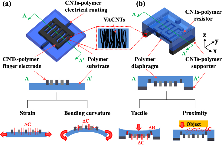
Figure 1. The designs and sensing mechanisms of the presented CNT-based flexible capacitive sensors: (a) strain sensor; (b) tactile/proximity sensor.
Download figure:
Standard imageFigure 2(a) shows the design parameters of the proposed interdigitated finger electrodes. With the bottom region of the CNT electrodes embedded into the polymer substrate (poly-dimethylsiloxane (PDMS) is adopted here), the initial capacitance (C0) of the sensor can be expressed as [13]

where pair and pPDMS are the dielectric constants of air and PDMS, h1 and h2 are the height of the interdigitated electrodes exposed to air and embedded in PDMS, respectively, a is the width of the interdigitated electrodes, w is the width of a finger, l is the length of a finger, d is the gap between finger electrodes and n is the number of interdigitated finger pairs. The height of the interdigitated electrodes determined by the CNT–PDMS composite could reach as much as nearly 50 μm. In comparison, a traditional metal thin film can only reach several microns. Thus, the initial capacitance and the sensing area are significantly improved by using the presented CNT–polymer electrodes. Table 1 summarizes the detailed dimensions of the proposed interdigitated electrode design. The initial capacitance of the sensor can be estimated as 1.2 pF according to equation (1).
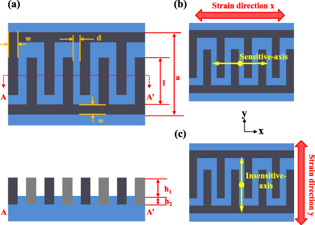
Figure 2. (a) Design parameters and (b)–(c) deformation in the sensitive-axis and the insensitive-axis of the proposed interdigitated finger electrodes.
Download figure:
Standard imageTable 1. The values of the design parameters of the proposed interdigitated finger electrodes.
| Symbol | Value | Symbol | Value |
|---|---|---|---|
| n | 8 pairs | pair | 1 |
| h1 | 50 μm | pPDMS | 2.75 |
| h2 | 20 μm | w | 50 μm |
| a | 1000 μm | d | 10 μm |
| l | 890 μm |
As the presented sensor is subjected to strain in the x-axis direction (sensitive-axis), a capacitance change will be caused by the gap variation between the finger electrodes, as shown in figure 2(b). The capacitance Cx of the sensor after being subjected to x-axis strain can be expressed as

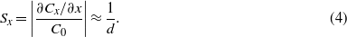
where x is the deformation in the sensitive-axis of the strain sensor. The sensitivity Sx (in the sensitive-axis) of the strain sensor can be expressed as

As the sensor is subjected to strain in the y-axis direction (insensitive-axis), a capacitance change will be caused by variation of the overlap length of the finger electrodes, as shown in figure 2(c). The capacitance Cy of the sensor after being subjected to y-axis strain can be expressed as

where y is the deformation in the insensitive-axis of the strain sensor. The sensitivity Sy (in the insensitive-axis) of the strain sensor can be determined as


From equations (4) and (7), the ratio of sensitivities between the sensitive-axis and the insensitive-axis is

From equation (8), with proper design of the interdigitated finger electrodes shown in table 1, the sensitivity of the strain sensor in the sensitive-axis is 88 times higher than that in the insensitive-axis.
In this study, finite-element method (FEM) analysis has also been employed to predict the capacitance change of the presented flexible sensor after loading. Since the CNT–polymer composites were composed of numerous discrete CNTs in a polymer matrix, it is complicated to establish the exact simulation model. Therefore, the CNT–polymer composite electrodes were simplified as homogeneous conductors in the simulation model to predict the performance of the presented flexible sensor. Figure 3 displays the simulation results for the capacitance changes as the sensor in figure 1(a) experienced four different loading conditions. The gap d between electrodes will be reduced as a compressive load is applied to the sensor in the x-axis direction (sensitive-axis). The gap shrinkage as well as compressive strain could be detected by the increase of capacitance change (ΔC) indicated by circular dots. One the other hand, the capacitance change is decreased (rectangular dots) when a tensile load is applied to the sensor. However, the sensor has no significant capacitance change (triangular dots) when subjected to loads in the y-axis direction (insensitive-axis). The simulation results demonstrate the sensing capability of presented sensor in the sensitive-axis, and also depict its ability to reduce the cross-axis signal induced by load in the insensitive-axis.
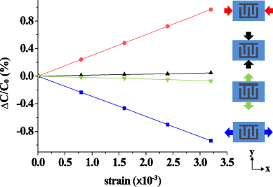
Figure 3. The FEM simulation results to show the variation of capacitance change with strain.
Download figure:
Standard imageThe simulation results in figure 4 indicate the variation of capacitance change with the tactile force for the presented sensor in figure 1(b). The interdigitated finger electrodes are located on the bottom of the PDMS diaphragm, while the tactile force applied on the top of the sensor. Because of the bending of the diaphragm, the gap between the finger electrodes will increase and further lead to a drop in the capacitance change, as shown in figure 4. This study also characterizes the performance of three different electrode heights (30,40,50 μm). The results indicate that the sensitivity would be increased with the height of the CNT–polymer composite electrodes.

Figure 4. The FEM simulation results to show the variation of capacitance change with tactile force.
Download figure:
Standard image3. Fabrication and results
Figure 5 shows the process steps (associated with the cross-sections AA' depicted in figure 1) to implement the proposed flexible capacitive sensor. As illustrated in figure 5(a), silicon dioxide was deposited and patterned to define the DRIE (deep reactive ion etching) regions. After that, Cr film was evaporated and patterned as the etching mask to define the supporter structures of the tactile/proximity sensor. As shown in figure 5(b), the photoresist was patterned to define the shape and gap of the finger electrodes, resistors, electrical routings and supporters. A first DRIE process was then employed to pattern the trenches of the supporters on the silicon substrate, as indicated in figure 5(c). After that, the Cr was removed by wet etching to open the finger electrode region. The height of the finger electrodes (about 50 μm) was determined by the trench depth after applying the second DRIE process, as shown in figure 5(d). Therefore, two different depths of the Si trenches for the supporters and finger electrodes would be implemented by such a two-step self-aligned DRIE process. The silicon substrate acted as a mold for the following processes. After that, a 10 nm thick Fe film was deposited and patterned by photoresist after the lift-off process on the silicon mold with a 3D surface, as exhibited in figure 5(e). The thin Fe film acted as the catalyst layer for the growth of CNTs. As illustrated in figure 5(f), the CNTs were grown by acetylene pyrolysis in a gas mixture of NH3 and C2H2 at 800 ° C for 15 min. CNTs of about 70 μm in height were grown in the regions with catalyst Fe film. Thus, the CNTs were properly filled in the trenches of different depths on the silicon mold and a highly structured 3D surface topography was achieved on the silicon substrate.

Figure 5. The batch fabrication processes, including (a)–(d) Si mold patterning, (e)–(f) 3D CNT growth and patterning, and (g)–(h) polymer molding.
Download figure:
Standard imageMoreover, a polymer molding process was exploited to form the polymer and CNT–polymer composite structures. In this study, PDMS (SYLGARD 184, base: curing agent =10:1, Dow Corning Co.) was employed as the polymer material for fabrication. Note that after the pyrolysis process for the growth of the CNTs in figure 5(f), the by-product of the amorphous carbon would coat on the surface of the silicon mold. This amorphous carbon would increase the adhesion between the PDMS and silicon, and make it difficult to de-mold the PDMS from the silicon mold. Therefore, O2 plasma was applied to remove the amorphous carbon before the following PDMS molding process. During the molding process, the PDMS was poured onto the silicon mold with 3D CNTs, as shown in figure 5(g), and the air trapped inside the trenches was fully removed by a vacuum pump. The molded PDMS attached to the mold–substrate was cured at 100 ° C for 1 h. After the de-molding process in figure 5(h), the PDMS and CNT–PDMS composite structures were manually peeled off by tweezers, and were released from the silicon substrate. The patterned CNTs, which acted as finger electrodes, resistors and the electrical routings for sensors, were transferred to flexible PDMS substrate. Other complicated 3D structures such as the polymer supporters to suspend the PDMS diaphragm for the tactile/proximity sensor were also realized. Note that the processes can easily change the dimensions of the CNT electrodes, and further tune the characteristics of the present flexible CNT capacitive sensor. Moreover, the dimensions (such as depth, width and aspect ratio) of the molded CNT–polymer structures are an important concern during the de-molding process. For example, the CNT–polymer composites could not be properly de-molded when the CNTs were grown on the Si mold with 10 μm-wide and 50 μm-deep trenches. On the other hand, the CNT–polymer composite could be de-molded when the trench width was increased to 20–50 μm. Further investigations are still required to determine the related issues.
The SEM micrographs in figures 6(a)–(b) display the top and cross-section views of the Si substrate patterned by DRIE with the patterned Fe catalyst. The silicon substrate with trenches, which acted as the mold for the CNT–polymer composite electrodes and supporter structures, is observed. With the aspect ratio hmold/wmold ∼ 1 of trenches shown in figure 6(b), the CNT–polymer composite could be successfully de-molded from the Si mold after the following molding process. Figure 6(b) also displays that the gap between two trenches shrank to 8.7 μm (the design value was 10 μm) due to over-development of the photoresist and sidewall etching in the DRIE process. After the acetylene pyrolysis process, the CNTs were filled in the trenches of the silicon mold, as displayed in figures 6(c)–(d). The interdigitated finger electrodes and electrical routings formed by the CNTs are clearly observed. Moreover, the CNTs resistors used to detect the contact of objects for the tactile/proximity sensor are also observed. Thus, the 3D patterned CNTs were successfully realized on the Si mold–substrate. The height of the CNT patterns grown on a single sensor was about 70 μm with a variation of approximately 5%, as shown in figure 6(d). The SEM micrographs in figures 6(e)–(f) further show more details of the proposed VACNT forest. The diameter of individual CNTs ranged from 90 nm to 116 nm, and the number density of the CNT film was about 3.6 × 1010 cm−2. The optical images in figures 7(a)–(b) show a typical fabricated silicon mold and the flexible sensor with a 5 × 1 sensing array after polymer molding, respectively. The CNT–PDMS composite (black) and the PDMS substrate (transparent) are observed in figure 7(b). The zoomed-in photos in figures 7(c)–(d) further show the fabricated flexible strain sensor and tactile/proximity sensor, respectively. The CNT interdigitated finger electrodes, resistors and electrical routings on the PDMS substrate can be observed. The polymer supporters indicated in the photo are achieved to act as spacers for the suspended diaphragm structure of the tactile/proximity sensor. The height of the CNTs grown in this study can be up to 70 μm. The figure shows that the CNTs can be easily filled into the trenches of the silicon mold to form 3D finger electrodes and further successfully transferred to the polymer substrate without any defect to realize the flexible capacitive sensor.
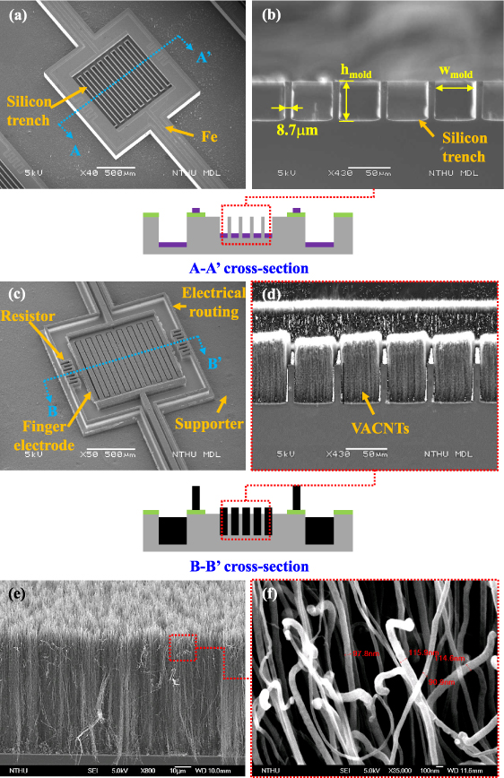
Figure 6. SEM micrographs of (a)–(b) top and cross-section views of the Si substrate patterned by DRIE with patterned Fe catalyst; (c)–(d) top and cross-section views of the CNTs filled in the trenches of the Si mold; (e)–(f) detailed views of VACNT forest.
Download figure:
Standard image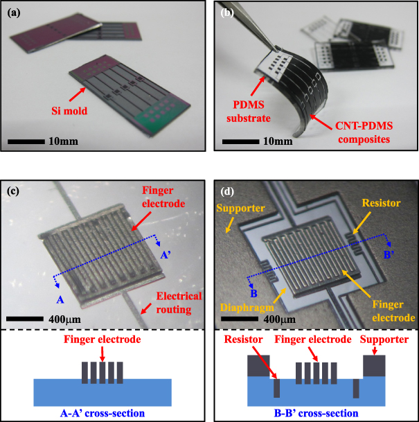
Figure 7. Optical images of (a) the fabricated Si mold, (b) the flexible sensor with a 5 × 1 sensing array and (c)–(d) zoomed views of the fabricated flexible strain and tactile/proximity sensors.
Download figure:
Standard image4. Experiments and discussion
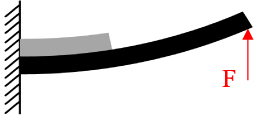
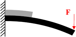
The experimental setup in figure 8(a) was established to demonstrate the application of the proposed strain sensor. A cantilever of length L and thickness t was mounted on a movable position stage. The position stage was employed to specify a displacement δ on the cantilever. The tip (free end) of the cantilever was initially contacted (not deformed) with a fixed sensing probe of a micro-force gauge (HF-1, ALGOL Engineering Co., with 1 mN resolution). Thus, the cantilever was bent by the sensing probe as the position stage moved upward. The tip deflection of the cantilever was specified by the displacement of the position stage δ. Meanwhile, the load on the cantilever was monitored by the force gauge. The strain sensor was adhered to the fixed end of a cantilever beam, and its strain εx can be expressed as

Thus, the strain εx of the test sensor was specified by the displacement of the position stage δ. When the sensitive-axis of the presented sensor was aligned with the x-axis, the bent cantilever caused a variation of the gap between the finger electrodes. On the other hand, the bent cantilever led to an area change of the finger electrodes when the insensitive-axis of the presented sensor was aligned with the x-axis. As a result, the strain of the bent beam was detected by the sensing capacitance change of the presented sensor and recorded by the LCR meter (E4980A, Agilent Technologies Inc.). Figure 8(b) shows the variation of the measured capacitance change (ΔC/C0) with the specified bending strain εx (the associated load applied to the beam increased from 0 mN to 700 mN). The gauge factor (GF) of the sensor is expressed as

where C0 is the initial capacitance. The presented flexible strain sensor had an initial capacitance C0 of 1.2 pF, which agrees well with the design value. In this case, the gap between the finger electrodes of the strain sensor was increased when the cantilever bent downward. Thus, the output capacitance of the strain sensor was decreased. On the other hand, as the cantilever bent upward, the output capacitance of the strain sensor was increased. When the strain was detected by the sensitive-axis of the sensor, the gauge factor and non-linearity of the bent-up case and bent-down case were 4.88 and 9.93% (circular dots), and 3.44 and 3.31% (rectangular dots), respectively. This study also rotated the strain sensor on the cantilever by 90°/270° to characterize its sensitivity in the insensitive-axis. The measurement results (triangular dots) in figure 8(b) show that the sensitivity of the strain sensor was significantly decreased in the insensitive-axis. These results agree well with the simulation results in figure 3 and also indicate that the variation of capacitance is mainly induced by the gap change of the finger electrodes. Table 2 summarizes the preliminary results for the strain sensor.
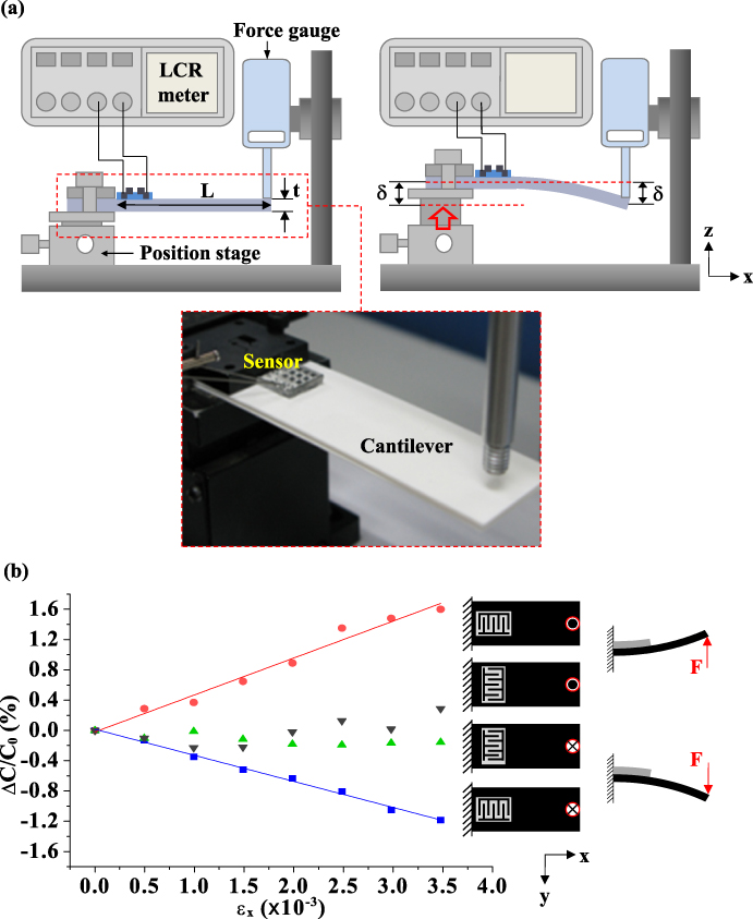
Figure 8. Measurements to show the variation of capacitance change with strain: (a) experimental setup; (b) measurement results.
Download figure:
Standard imageTable 2. Measurement results for the strain sensor.
| Side view |
|
|
||
| Top view |

|

|

|

|
| Gauge factor (ΔC/C0/εx) | 4.88 | — | 3.44 | — |
| Non-linearity (%) | 9.93 | — | 3.31 | — |
However, the capacitive sensitivity of the measurement results (GF = 3.44–4.88) in figure 8(b) is higher than that of the simulation results (GF = 3) in figure 3. The difference could be due to the strain sensor being subjected to different loading conditions between the simulation and the experiment. For example, as shown in figure 9(a), when the sensor was subjected to tensile load in simulation, the gap dx between the finger electrodes was increased by the axial strain εx,

where d0 is the initial gap between the finger electrodes. However, when the strain sensor was adhered to the fixed end of a bent cantilever in the experiment (shown in figure 9(b)), not only the axial strain εx but also the radius of curvature ρ of the strain sensor would increase the gap between the finger electrodes. The equivalent extended gap deq between the finger electrodes can be obtained as


where h1 is the height of the finger electrodes. According to equation (13), the equivalent extended gap deq in the experimental conditions is larger than the extended gap dx in the simulation conditions (deq > dx) under the same tensile strain εx. From equation (1), the variation of capacitance change in simulation (ΔCs/C0) and in experiment (ΔCe/C0) can be respectively determined as


By replacing dx and deq in equations (14) and (15) with equations (11) and (13), the ratio of gauge factors between experiment (GFe) and simulation (GFs) can be expressed as

When the height of the finger electrodes h1 is 50 μm and the radius of bending curvature of the strain sensor ρ is 0.21 mm in the experimental conditions, the sensitivity of the measurement results would be 1.03 times higher than that of the simulation results by equation (16). Moreover, the initial gap between the finger electrodes of the strain sensor was shrunk due to variation in the manufacturing process (e.g., over-development of the photoresist and sidewall etching in the DRIE process). This is also a critical concern as it causes the measurement results to be higher than the simulation ones. Figure 6(b) shows that the initial gap between the CNT finger electrodes (the gap between Si trenches) was shrunk to 8.7 μm. Compared with the designed gap of 10 μm in the simulation model, the sensitivity of the measurement results would be about 1.15 times higher than that of the simulation ones according to equation (4). Furthermore, the simplified simulation model of CNT–PDMS composites may also influence the variation between the simulation and measurement results.

Figure 9. Different loading conditions imposed on the proposed strain sensor: (a) in the simulation conditions; (b) in the experimental conditions.
Download figure:
Standard imageThe experiment setup in figure 10(a) was established to measure the profiles of the interdigitated electrodes and the output capacitance of the sensor at different bending curvatures. Round stages of four different curvatures were prepared. The presented flexible CNT sensor was fixed to the stage so as to specify its bending curvature. The profiles of the interdigitated finger electrodes were measured by the optical interferometer and the output capacitance of the strain sensor at different bending curvatures was recorded by the LCR meter. Figure 10(b) displays the measured initial surface profile of the finger electrodes. The height of the finger electrodes determined by DRIE is observed. Figure 10(c) further depicts the measured surface profile of the finger electrodes when the sample was fixed to a round stage with a 20 mm radius of curvature. Due to the specified bending deformation shown in figure 10(a), the gap between the CNT–polymer finger electrodes is increased. As indicated in the illustration in figure 1(a), the output capacitance of the strain sensor is decreased. The measurements in figure 10(d) indicate that the capacitance change was decreased by about 12% when the curvature increased from 0 mm−1 to 0.08 mm−1.

Figure 10. Measurements to show the profiles and variation of capacitance change with bending curvature: (a) experimental setup; (b) initial surface profile of the finger electrodes; (c) bending surface profile of the finger electrodes; (d) capacitance change with bending curvature.
Download figure:
Standard imageThe measurement setup in figure 11 was established to characterize the performance of the presented CNT-based flexible tactile/proximity sensor. The sensor (with a span of 1.6 mm between the two supporters) under testing was fixed to a position stage, and the stage height was tuned to move the sensor upward to the force gauge. When the sensor approached (but did not contact) the probe of the force gauge (with a diameter of 5 mm, also acting as the sensing object), the fringe capacitance of the interdigitated electrodes would be influenced. Thus, the presented sensor acted as a proximity sensing device to detect the distance between the sensor and the sensed object through capacitance change. After further moving the position stage upward, the force gauge would contact the sensor and then apply a normal load to deform its suspended diaphragm. As illustrated in figure 1(b), deformation of the diaphragm led to a capacitance change of the interdigitated electrodes and a resistance change of the CNT resistors. In this regard, the presented sensor became a tactile sensing device to detect the tactile force on the sensor through capacitance change. Note that the resistance change of the CNT resistor was to confirm the contact of an object. The sensing signals of the CNT interdigitated electrodes and CNT resistors were recorded by the LCR meter. The typical measurement results in figure 12 show the tactile and proximity sensing characteristics of the presented sensor. The measurements in figure 12(a) depict the variation of resistance and capacitance change with the distance D between the force gauge tip and the sensor surface (as indicated in figure 11(a)). The distance D < 0 represents the situation after the contact of the force gauge and the sensor. During the proximity sensing (when D > 0), the sensing capacitance decreased from 2.62 pF to 2.60 pF when the object approached from D = 90 to 0 μm. (Note that the change of sensing capacitance was 76 fF when an object approached with D = 2 mm.) With regard to the tactile sensing (when D < 0), the sensing capacitance decreased from 2.60 pF to 2.51 pF when the object moved from D = 0 to −30 μm. The measurements also indicate that the capacitance change of proximity sensing caused by the fringe effect of the interdigitated electrodes was much smaller than that of tactile sensing. Moreover, figure 12(a) shows that the resistance of the CNT resistor is not changed until the contact of the object. This characteristic demonstrates the capability to confirm the contact of the sensed object and to distinguish the proximity and tactile sensing modes for the sensor. Figure 12(b) further shows more details of the tactile force measurement results recorded from the force gauge. The variation of the capacitance change was decreased by about 1.6% when the tactile force increased from 0 to 1600 mN. As a result, the presented sensor has a tactile force sensitivity of 1.11% N−1.

Figure 11. The measurement setup for applying proximity distance and tactile force to the packaged flexible capacitive sensor.
Download figure:
Standard image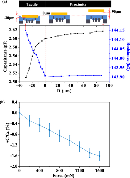
Figure 12. Measurements to show (a) the variation of capacitance and resistance change with the distance D between the force gauge tip and the sensor surface, and (b) the variation of capacitance change with tactile force.
Download figure:
Standard image5. Conclusions
In summary, this study has successfully demonstrated a simple molding approach to enable the integration of patterned 3D CNTs with polymer, and further implement a CNT-based flexible capacitive sensor. A silicon substrate patterned by DRIE is employed as the mold for CNT growth and the following polymer molding. Thus, 3D CNT patterns are easily grown and defined on the silicon mold, and then embedded into a polymer to implement the flexible sensor. The CNTs grown on the silicon mold are up to 70 μm in height, and the CNT–polymer interdigitated finger electrodes defined by the trench depth are about 50 μm. Such tall finger electrodes can increase the capacitance sensing area with a higher initial capacitance and sensitivity. Various mechanical structures can also be achieved using the 3D CNT–polymer composite. In applications, two flexible capacitive-type sensors including a strain sensor and a tactile/proximity sensor are demonstrated and tested. The 3D CNT–polymer composite is successfully exploited to realize the finger electrodes, resistors, electrical routings and supporter structures in these sensors. Measurements show that the gauge factors of typical fabricated strain sensors are in the range of 3.44–4.88 (non-linearity range of 3.31%–9.93%) and the sensitivity of the tactile sensor is 1.11% N−1. Moreover, the sensor could also detect the proximity of objects approximately 2 mm away from the sensor. However, the influence of the CNT properties (diameter, height and number of CNTs) on the sensor sensitivity has not been investigated. This could be an important topic for future work.
Acknowledgments
This paper was partially supported by Brain Research Center at National Tsing Hua University, and by the National Science Council, Taiwan, under contracts 100N2060E1, 100N7049E1 and NSC 99-2221-E-007-040-MY3. The authors would like to express their appreciation to the Center for Nanotechnology, Materials Science, and Microsystem of the National Tsing Hua University, the Nano Facility Center of National Chiao Tung University and the Nano-Electro-Mechanical-Systems Research Center of the National Taiwan University for providing fabrication facilities.