

Abstract
We investigated dependence of the dielectric properties on temperature and electric field below 50 K along the chain direction of o-TaS3. With external electric field increase, two threshold features could be identified. For electric fields somewhat larger than the lower threshold  , the dielectric constant starts to decrease whereas the conductivity increases due to the tunnelling of solitons. For higher external electric field we observe a saturation of dielectric response and analyze that the possible reasons may be related to the polarization behavior of charged solitons. With a decrease in temperature, the effect of external field on the dielectric response of the system weakens gradually and at 13 K it diminishes due to soliton freezing.
Export citation and abstract BibTeX RIS
1. Introduction
The charge density wave (CDW) is a periodic distribution of conduction electrons in real space, accompanied by a crystal lattice distortion. It is usually observed in a wide class of quasi-one-dimensional (Q1D) solids below the Peierls transition temperature (TP) [1–3]. There has been considerable progress in the understanding of the macroscopic carrier condensate in connection to CDW phase solitons [4–11].
Solitons allow for hopping between different ground states. Since the energy levels of these states are very similar, the excitation energy of the charged particles would be lower than the bare electronic gap. CDW phase solitons are the excitations of topological phase defects whose presence has long been expected in Q1D systems [12–14]. More than three decades ago, Su et al showed that excitations (solitons) with fractional charges may exist in half-filled or one-third-filled Peierls systems [13, 14]. In [9], x-ray data indicated possible internal degrees of freedom of the CDW solitons. Moreover, the experimental results from optical methods obtained by Zaitsev-Zotov et al convincingly supported the existence of solitons in orthorhombic TaS3 (o-TaS3) [5]. Further, in very recent experiments, the charged phase solitons have been directly observed in NbSe3 by Brun et al using scanning tunnelling microscopy [15]. In an idealized CDW system the spacial arrangement of the density of conduction electrons would have a perfect period, but in a real crystal there are defects distributed randomly in phase field (CDW phase solitons). As the CDW phase is the manifestation of the charge density distribution, the excitations of phase solitons should respond to the external electric field.
In [10], two thresholds in field dependent conductivity ( ) were identified below 60 K in TaS3. The lower
  was proposed to be related to solitons, whereas above 100 K there was only one threshold due to the classical CDW depinning. The polarization process activated below about 70 K, was also attributed to solitons (localized pinned CDW excitations) [16]. A new phase diagram was suggested where the Coulomb blockade threshold lower than the classical CDW depinning threshold field
  emerges for charge soliton nucleation [17, 18]. Furthermore, a new ac–dc interference spectrum in the differential conductivities of o-TaS3 were observed, attributing the driving force to the depinning of solitons [6]. Solitons contribution therefore could be rather important for the charge dynamics of CDW.
o-TaS3 is a typical quasi-one-dimensional semiconducting CDW material with the  K, below which a temperature dependence of the linear conductivity obeys the activation law with an activation energy
  K. At
K. At 
 , the linear conductivity begins to deviate from the activation law with a smaller activation energy, indicating possible excitations of charged solitons [10]. Considering that the lower threshold
  is possibly related to the pinned or bounded solitons, in this work we investigate charge transport and dielectric properties in external electric field
  .
.
Temperature dependent complex dielectric or conductivity spectrum is a powerful probe for studying charge dynamics [4, 19–22]. At a fixed temperature T0, the complex dielectric spectrum of a material  is ultimately defined by the polarizations of the corresponding charged microscopic particles. In CDW systems exceptionally large dielectric constants and strong dispersion effects below 105 Hz were observed [16, 23–25]. Further, under various E established by dc bias, dielectric spectroscopy would be of great interest since the collective transport or the solitons excitations in CDW systems could only occur above the threshold. In order to study CDW dynamics and to eliminate the screening effect of the normal electrons excited through the Peierls gap, experiments should be carried out at a much lower temperature. To the best of our knowledge the bias dependent dielectric response below 50 K has been inadequately reported for TaS3. Zhilinskii et al observed that the dielectric constant did not change in o-TaS3 even up to 100 V cm−1 at 4.3 K though the conductivity increased [11]. However, the evolution of the dielectric behavior under external field covering
  below T = 50 K has not been studied and is of interest.
Here we studied the temperature and electric field dependent charge dynamics along the chain direction of o-TaS3 below 50 K. With increasing the external electric field, two threshold-like features could be identified. For fields larger than  , the dielectric constant starts to decrease while the conductivity increases due to the tunnelling of solitons. As E continues to increase, there is a saturation of dielectric response. With decreasing temperature, the effect of the external field on the dielectric responses of the system weakens gradually, and at 13 K it diminishes.
2. Experiments
TaS3 crystals were successfully grown by the conventional chemical vapor transport method. The stoichiometric tantalum and sulfur pieces were put into an alumina crucible before sealing in a quartz tube and reacting at 700 °C for 50 h. Single crystals were grown by vapor transport method in a gradient furnace. The temperature of hot (cold) end was 700 °C (500 °C). Consistent with the earlier reports [26], the as-grown single crystals showed thin needle-like shape with dark black color, typical sizes with diameter about 25  m and length up to 10.0 mm. In the experiments, we focused on the axis direction of the sample, which is corresponding to the chain direction of o-TaS3 [2].
Temperature dependent resistivity was measured with current I = 10  A before probing the dielectric spectrum by four-terminal-pair approach. The I–V curves showed linear behavior, confirming good ohmic contacts by Indium compression6. We also compared the contact resistance of the 4-contact with 2-contact probe and found the difference was negligible from 300 K to 12 K. In addition, we confirmed that the impedance spectra were unaffected by the difference between substrates by comparing data obtained with the LaAlO3 and sapphire. The complex impedance properties under sweeping dc bias
  from 0 to 50 V cm−1 were probed on Agilent 4294A precision impedance analyzer through four-coaxial cables in two pairs (corresponding to two electrodes on the sample), where
  was the phase difference between the ac potential and current at frequency ω. The sample was mounted on a cryostat with the experimental temperature range 13–300 K. All the impedance spectra were measured with driving voltage Vp−p = 30 mV(rms), far below the electric threshold field obtained in I–V measurements. In analysis, the sample was a leakage capacitor, both dielectric constant
  and the complex conductivity spectrum
  could be deduced from the raw data
  based on the universal relations:
  , where
  (i = 1,2), d and S were the length and the cross-sectional area of the sample, respectively.
3. Results and discussions
The temperature dependent resistivity  (T), the Peierls transition temperature
  K, I–V relations and
  from 300 K to 13 K along the chain direction of o-TaS3 crystal were all consistent with previous results [9, 10]. Here we showed the
  curves below 60 K since it is the interesting temperature range, see figure 1. The lower threshold
  could be clearly seen below 50 K, whereas
  would be up to a much larger value7. In our experiment,
  V cm−1 at T = 20 K, whereas
  V cm−1 at 4.3 K in [10].

Figure 1. Bias dependent conductivity of o-TaS3 crystal (normalized by  , the conductivity at 300 K) at various temperatures below 60 K. The dashed line expresses the lower electrical thresholds at corresponding temperatures,
  .
.
Download figure:
Standard image High-resolution imageBefore studying the dielectric properties under external dc electric field E, we probed the temperature dependent dc conductivity shown in figure 2(a). Below T = 60 K, the log reveals a linear behavior and the activation energy obtained is about
  K, whereas above T = 100 K, the activation energy is about
  K, in agreement with the earlier reports [10]. The dielectric spectra under zero external field are shown in figures 2(b) and (c), from which it could be seen that the evolution of the polarization characteristics with temperature is very similar to [16]. At T = 185 K, with the establishment of the CDW, one relaxation process emerges at higher frequencies. The peak of the imaginary part of the dielectric spectrum shifts towards low frequencies with decreasing temperature, indicating the gradually freezing of this process, as shown by the arrows marking in figure 2(c). At T = 77 K and below, another process appears at higher frequencies as denoted by the double arrow. To be consistent with [16], we call the first process α and the second one β. Clearly, at T = 50 K, the α process due to the elastic pinned CDW screened by uncondensed carriers shifts out of the measurable frequency window and the β process which was attributed to solitons (localized pinned CDW excitations) dominates the charge dynamics [16]8. These two processes under dc field E = 0 were systematically investigated in [16].

Figure 2. (a) Logarithm of conductivity versus inverse temperature of o-TaS3 crystal (normalized by  with the Peierls transition
  K. The dashed and dotted lines are guided to the eyes. (b) and (c) The real and imaginary part of the temperature dependent dielectric spectra of the same TaS3 crystal as (a). Note that the arrows in (c) are shown for the α processes, whereas the double-arrows denote the β processes.
Download figure:
Standard image High-resolution imageIn order to investigate the charge dynamics in current carrying states, we probed the dielectric properties by sweeping dc bias below T = 50 K. Corresponding to the lower threshold  in conductivity, for example, at T = 35 K as shown in figures 3(a) and (b), the
  curve starts to decrease. Above this threshold, at about Es = 7.0 V cm−1, the relation of
  tends to saturate. Clearly, Es is larger than
  but much smaller than
  V cm−1 at T = 35 K. To the best of our knowledge, such a decrease and then saturation in field dependent dielectric constant has not been reported yet.
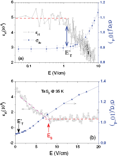
Figure 3. (a) (left) The bias dependent dielectric constant of o-TaS3 crystal at f = 1.0 kHz and T =35 K. (right) The normalized conductivity along the chain direction of o-TaS3 crystal. In order to clarify the features near  , the data were shown in a logarithm of the external electric field. (b) Similar to (a) but shown in a linearity of the external electric field, in order to clarify the features near E = Es. The dashed lines are guides for the eyes.
Download figure:
Standard image High-resolution imageGenerally, the structural defects can be polarized under dc field with a smooth dielectric response, hence the experimental data excludes this possibility. Considering that the β process (dynamics of solitons pinned at impurities) would dominate the charge dynamics below the freezing temperature of the α process and that the activation energy  K obtained above is consistent with the existence of a band within CDW gap, we propose that the main feature in electronic polarization properties of the
  -TaS3 crystal may originate from trapped or pinned CDW phase solitons [27–29].
The presence of CDW phase solitons has been convincingly shown in  -TaS3 [5, 6, 9, 15]. As the phase of CDW presents the distribution of the charge density in the real space, it is plausible that the phase defects would response to the external electric field. In zero field limit, all pinned solitons could be polarized and contribute to the dielectric constant. In figure 4(a), the electronic polarization of charged solitons presents as a small displacement (solid bell shaped curve shifts somewhat from the dashed curve) in external dc field.
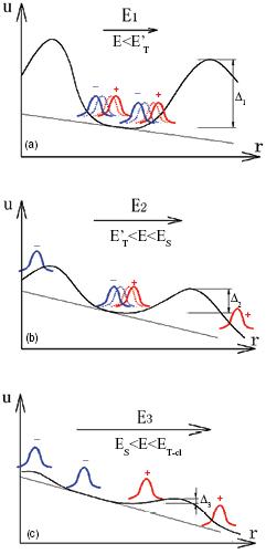
Figure 4. (a)–(c) The schematic pattern of solitons (shown by small peak-like curves) tunnelling under various dc bias. The external electric field from (a) to (c) gradually increases, correspondingly, the potential barrier decreases. The label of the horizontal axis r presents the position of the real space whereas for the vertical axis, u presents the potential energy. Note that the pair of dashed-solid curves (red for positive charged solitons while blue for negative charged solitons) present the electronic polarization of the pinned solitons. Only the solitons in potential well are localized.
Download figure:
Standard image High-resolution imageWith increasing E the increasing conductance corresponds to a decreasing dielectric constant. We suggest that only the pinned solitons could be locally polarized and the others could tunnel through the energy barrier with the help of external field. Hence the real part of the dielectric constant decreased with increasing external electric field, see figure 4. Having in mind that the CDW phase solitons are the phase defects, then electronic polarization could occur locally around the equilibrium positions of the solitons in the potential well under external field. As expected, if the reduction of the real part of the dielectric constant is caused by the tunneling of the phase solitons, the imaginary part of dielectric constant  must increase. Indeed, we observed such behavior, see figure 5(a). When E is increased further, it is plausible that more and more solitons would be depinned and eventually the contribution to polarization from pinned solitons would diminish and the dielectric constant saturate. Corresponding to this saturation in
  or the delocalization of the whole trapped solitons,
  turns downward above Es, revealing a change in the mechanisms of energy loss, see figure 5(a). In very recent reports, Matsuura et al proposed soliton liquid model to interpret the observed ac–dc interference spectrum [6]. Here we suggest that the main contribution for the observed features in the dielectric properties may come from the charged phase solitons in o-TaS3.
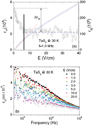
Figure 5. (a) The bias dependent dielectric constant at f = 1.0 kHz and T = 30 K. The dashed line on the figure is a guide for the eyes and shows the saturation tendency with increasing electric field. The thick black solid line presents for Es, above which the real part dielectric constant saturates. (b) The dielectric spectra at various dc bias and T = 30 K. Note that the dielectric response is dependent to the lower external electric field whereas independent above E = 10.0 V cm−1.
Download figure:
Standard image High-resolution imageWith decreasing temperature, the kink feature in  weakens. For example, at 30 K, see figure 5(a), the dielectric constant starts to decrease to E = 8.0 V cm−1 and then it saturates at about
  from E = 8.0 V cm−1 to 40.0 V cm−1. The difference between the saturation field and the zero-limit field
  decreases when compared to T =35 K. In figure 5(b), the frequency dependent dielectric spectra under various dc bias are shown. The obvious feature in figure 5(b) is that the β relaxation process becomes suppressed as most pinned solitons tunnel through barriers under larger electric fields. For example, the difference of the dielectric response at E = 10.0 V cm−1 and E = 20.0 V cm−1 can not be identified within the experiment error. With further cooling, at 13 K the kink is nearly negligible, as shown in figure 6(a), the dielectric constant only increases slightly in lower frequency region below several kHz at E = 50 V cm−1. The spectra remains nearly unchanged up to 1.0 MHz below 40 V cm−1, see figure 6(b), indicating bias independent dielectric properties in moderate electric field.
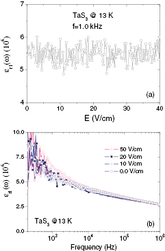
Figure 6. (a) The bias dependent dielectric constant at f = 1.0 kHz and T = 13 K. (b) The dielectric spectra at various dc bias and T = 13 K. Note that the dielectric response is nearly independent to the external electric field below E = 50 V cm−1.
Download figure:
Standard image High-resolution imageThe temperature dependent  has been shown in figure 7. From this tendency, it is natural that the dielectric response would remain constant with increasing electric field at liquid helium temperatuare [11]. The diminished
  may originate from the freezing of β relaxation process. Meanwhile this is consistent with the model proposed by Matsuura et al, that the number of solitons are determined by the electron density [6, 9]. Below 50 K the lower threshold field
  decreases with decreasing temperature. This can be explained based on the relation that the dielectric permittivity multiplied by the threshold field should be a constant, regardless of the details of the pinning mechanism of the CDW [16].

Figure 7. (left) the temperature dependent dielectric constant difference at 1.0 kHz; (right) the temperature dependent  . Note that above 16 K, the β process dominates the dielectric properties of the system [16].
Download figure:
Standard image High-resolution imageAs shown in figure 7,  decreases with decreasing temperature, possibly indicating that the density of solitons would decrease with cooling. Such a phenomenon might be related with the reports from [9], in which the commensurate CDW develops with a decrease of temperature. Nevertheless, research work about the dynamics of solitons in TaS3 is not sufficient up to date, especially at temperatures below T = 50 K. The qualitatively similar behavior between
  and
and  reveals that the ease for solitons tunnelling diminishes the dielectric constant of the system. In this tendency, the β process would be replaced by the
  process [16]. Based on our experimental data at T = 13 K, it seems that the
  process is not related to the locally pinned solitons since its independence to the external electric field. Then one may ask the reason for the essential increase of conductivity with increasing electric field at T = 13 K. In previous report [11], Zhilinskii et al also reported that the similar results: the real part of the dielectric constant
  remained unchanged at dc fields of about 100 V cm−1 (T = 4.3 K), while the conductivity increased by several times. Here we suggest that the freezing of one process means that the electronic polarization can not respond timely to the ac external field at a finite frequency, while for the dc field, the hopping mobility of the excited solitons may increase nontrivially and hence the conductivity increases.
4. Summary
In summary, we measured the dependence of the dielectric properties of TaS3 crystals on temperature and electric field. Below T = 50 K, the electrical threshold  in I–V curve could be clearly identified. Above
  , with increasing E, the dielectric constant starts to decrease while the dc conductivity increases due to tunnelling of solitons. The saturation of the field dependent dielectric constant was suggested to occur when the solitons could no longer be polarized locally under a field E > Es. With further cooling, the threshold
  decreases and the difference of the dielectric constant between the saturation and the zero-limit field value
  also decreases due to soliton freezing.
Acknowledgments
The authors are very grateful for instructive discussions with Toru Matsuura. The research work was supported by the National Science Foundation of China (Grant No. 10704054). Work at Brookhaven National Laboratory is supported by the US DOE, Contract No. DE-SC00112704.
Footnotes
- 6
For the measurements of the transport properties, the electrodes would be used as contacts to the samples. Usually, the silver paste and cold-soldered indium could be used. In our experiments, the indium electrodes (which were compressed by clamps) contact the CDW sample and the conduction wires.
- 7
For calculating the threshold
 , firstly, we observed the tendency of the curve and found that the conductivity monotonically increases with E. Then if (the experiment error), the value E = Ex would be adopted to be the . Finally, we showed the s at various temperatures in figure 1 (the dashed curve shows that with decreasing temperature, decreases, which is in consistent with [16]).
 - 8
Two models of the β process are discussed to explain the experimental data in [16]. One model requires the screening of solitons by the free carriers. The other approach, based on the idea of the hopping of the solitons between the impurity sites, has also been proposed. It relies on the theory of the ion hopping in glasses.


![$\left[\sigma \left(E={{E}_{x}}\right)-\sigma (E=0)\right]/\sigma (E=0)>5\%$](https://content.cld.iop.org/journals/0953-8984/28/39/395901/revision1/cmaa314cieqn069.gif)


