
Abstract
The electron–phonon coupling parameters in the vicinity of the
 point,
 , for electronic quantum well states in epitaxial lead films on a Si(1 1 1) substrate are measured using 5, 7 and 12 ML films and femtosecond laser photoemission spectroscopy. The
values in the range of 0.6–0.9 were obtained by temperature-dependent line width analysis of occupied quantum well states and found to be considerably smaller than the momentum averaged electron–phonon coupling at the Fermi level of bulk lead, (λ = 1.1–1.7). The results are compared to density functional theory calculations of the lead films with and without interfacial stress. It is shown that the discrepancy can not be explained by means of confinement effects or simple structural modifications of the Pb films and, thus, is attributed to the influence of the substrate on the Pb electronic and vibrational structures.
, for electronic quantum well states in epitaxial lead films on a Si(1 1 1) substrate are measured using 5, 7 and 12 ML films and femtosecond laser photoemission spectroscopy. The
values in the range of 0.6–0.9 were obtained by temperature-dependent line width analysis of occupied quantum well states and found to be considerably smaller than the momentum averaged electron–phonon coupling at the Fermi level of bulk lead, (λ = 1.1–1.7). The results are compared to density functional theory calculations of the lead films with and without interfacial stress. It is shown that the discrepancy can not be explained by means of confinement effects or simple structural modifications of the Pb films and, thus, is attributed to the influence of the substrate on the Pb electronic and vibrational structures.
Export citation and abstract BibTeX RIS
1. Introduction
Understanding the interaction of electrons and phonons is of fundamental interest in basic research as well as in applied science, in particular for nanoscale- and confined systems. This interest arises mainly from the effect of electron–phonon coupling (EPC) on macroscopic material properties that often results in device design limits, e.g. conversion efficiency limits in photovoltaics or waste heat generation in nanoscale electronic devices. For example, the electric conductivity is strongly influenced by, e.g. the formation of a superconducting condensate, a metal to insulator transition [1] or spatial confinement effects that reduce resistivity due to phase-space restrictions for scattering events, e.g. in graphene [2, 3].
While a detailed discussion of EPC processes must remain problem-specific, it is useful to quantify EPC by means of a single parameter, regardless of the underlying microscopic processes. EPC is often being quantified through the dimensionless parameter λ commonly used in the theory of conventional superconductivity. This parameter can be studied by means of a variety of methods from both the experimental and the theoretical side. Common experimental techniques include scanning tunnelling spectroscopy, photoemission spectroscopy or the determination of critical temperatures in superconductivity. Theoretically, λ can be derived by summing up the manifold of possible electron–phonon scattering events, being either formulated by means of momentum or energy transfer [4].
While EPC in bulk metals is well understood, low-dimensional systems might exhibit strong confinement effects as structure sizes decrease and the material's surface or interface contributions become more important [5–12]. In addition, the coupling of the confined system to a meso- or macroscopic environment becomes significant as new scattering and transport channels emerge. To investigate such effects, the Pb/Si(1 1 1) film-substrate system with its confined electronic structure and tunable discrete electronic density of states is an optimal candidate.
Up to now most studies were focused on superconducting properties of the system, specifically, on the critical transition temperature [17–22]. The reported values of Tc in ultrathin Pb(1 1 1) films grown on a Si(1 1 1) substrate, Tc = 1.8 − 6 K, are smaller compared to the value for bulk Pb, Tc = 7.2 K, thereby raising the question whether confinement or interfacial effects reduce the EPC. Density functional theory (DFT) calculations [23, 24] showed that the critical transition temperature in free standing Pb(1 1 1) films is higher than Tc obtained from the measured gaps in Pb(1 1 1) films grown on a Si(1 1 1) substrate and agrees well with the experimental bulk value [24]. Unfortunately, the theoretical studies highlighting the complexity of the problem could not include direct ab initio calculations of the influence of a substrate that should obviously be important for such small thicknesses. In addition, all these studies both theoretical and experimental are focused on the properties that are governed by λ(EF), a momentum-averaged quantity evaluated at EF, that is modified by interfacial/thin film effects in a very complex way, e.g. when the sample dimensions become comparable to the electron coherence length [25]. To shed light on the influence of confinement and the film-substrate interface on EPC, a detailed investigation of electron–phonon interaction in particular electronic states could be advantageous, but is missing.
Such a detailed analysis of individual electronic states allowed by photoemission spectroscopy provides a direct access to EPC. Zhang et al [29] found the reduced EPC parameter in electronic quantum well states (QWS) to be in the range of λ = 0.6–1.0. While a possible implication of interfacial stress effects was tentatively suggested, a detailed conclusion on the origin of the strongly suppressed EPC remained elusive. In addition, the reported data concern rather thick Pb films on Si(1 1 1), 15–24 ML. We take up these experiments by combined theoretical and experimental studies on thinner films, in which interface and/or confinement effects are expected to be more pronounced.
In this work, the electron–phonon coupling in occupied electronic quantum well states of ultrathin Pb films epitaxially grown on a Si(1 1 1) substrate is investigated. Experimental values of
(at the
point) for 5, 7 and 12 ML Pb films are obtained by temperature-dependent photoemission line width analysis using 6 eV photons from a femtosecond laser source. This technique allows for a determination of λ with a reduced surface sensitivity, ensuring the investigation of the entire Pb thin film properties [13, 14]. The experimental results are directly compared to DFT calculations with and without taking into account interfacial stress. Significant differences found in the EPC strength can not be explained by means of confinement effects or simple structural modifications of the Pb films and, thus, are attributed to the influence of the substrate on the Pb electronic and vibrational structures.
2. Material and methods
2.1. The Pb/Si(1 1 1) quantum well state system
Pb exhibits a rather large Fermi-wavelength for electronic states along the Γ−L direction [26, 27], that gives rise to the formation of sharp occupied and unoccupied electronic quantum well states in epitaxial thin films grown on Si(1 1 1) substrates that have been intensely studied by experimental and theoretical methods (see, e.g. [16], [17], [19], [26–30]). Considering the phase-accumulation model, electrons within the Pb film are confined by the vacuum and the Pb/Si interface barrier such that the electron wave function has to obey the Bohr–Sommerfeld quantization rule:

where k(E) denotes the wave number for energy E, Θ is the number of monolayers with interlayer spacing d = 2.86 Å, n is a quantum number and ΦV/Si(E) are the energy-dependent phase shifts upon reflection from the vacuum and the Si interface, respectively. This quantization leads to an almost commensurate period of ΔΘ ≈ 2 ML for electronic states in the vicinity of the Fermi energy, resulting in different branches of QWS that approach and finally cross the Fermi level with increasing film thickness. For 5, 7 and 12 ML film thickness, intense occupied QWS are observed which are energetically fully degenerated with the Si band gap [31] and, thus, spatially confined to the film. As a consequence for our experiments, no contribution from wave-function delocalization or hybridization to photoemission line-width can be expected, making these states the ideal test candidates to study EPC. On the other hand, additional line width broadening prevents detailed studies of EPC for other film thicknesses, where aforesaid conditions are not fulfilled.
2.2. Experimental setup and sample preparation
Epitaxial Pb films were grown under ultrahigh vacuum conditions in a three-step process: First, the Si(1 1 1)-(7 × 7) surface reconstruction was prepared and subsequently saturated by establishing the Si(1 1 1)-
 -Pb(β) surface reconstruction. Finally, additional Pb was evaporated from a Knudsen cell and epitaxial Pb(1 1 1) films were grown in a wedge geometry with a typical thickness gradient of 0.5 MLmm−1 along the 26 mm wide Silicon substrate. The use of continuous lead wedges facilitates the investigation of several film thicknesses in a single experiment and compensates for uncertainties in the evaporation rate of the Knudsen cell. The sample temperature was held constant at T = 100 K during the deposition process to avoid formation of islands due to atomic diffusion. Film thicknesses were cross-checked after deposition by comparison of the electron binding energies with earlier experimental work and DFT calculations [16]. The surface structure in each preparation step was monitored using low energy electron diffraction (LEED). For further details on sample preparation see [13, 28].
Femtosecond laser pulses from a commercial Ti:Sapphire system operating at 250 kHz repetition rate and a central wavelength of 800 nm (1.55 eV) were frequency quadrupled (6.2 eV) in two consecutive β-BaB2O4 crystals and used for direct photoemission. The p-polarized pulses were focused to a spot size of (45 µm)2 and incident on the sample under an angle of 45° with respect to the (1 1 1)-surface normal, ensuring photoemission from a well-defined layer thickness (ΔΘ = ±0.01 ML along the beam profile) on the continuous wedge film 7. The laser intensity was carefully tuned to prevent spectral broadening due to space-charge effects, resulting in typical electron count rates of 150 kHz at the electron detector.
While the finite spectral width (52 meV) of our laser pulses does not allow for high-resolution photoemission experiments, laser-based photoemission with 6.2 eV photon energy offers several advantages compared to more frequently used light sources like, e.g. He discharge lamps. Beside the possibility to perform femtosecond time-resolved experiments, laser-based photoemission combines a high photon flux with an increased bulk-sensitivity [14], as recently demonstrated in experiments under similar conditions where hybridized electronic states at the Pb/Si(1 1 1) interface were observed even for 1.4 nm Pb film thickness [13].
Photoemission spectra were recorded at different temperatures in normal emission geometry using an electron time-of-flight analyzer with an acceptance angle of ±3.8° and an energy resolution of 25 meV. The finite momentum resolution (0.03 Å−1 at a typical electron kinetic energy of 1.5 eV) does not significantly contribute to the measured line width due to the high effective masses of the localized pz-like orbitals under investigation here [30, 32, 33]. Summarizing, the overall spectral resolution was estimated to be 65 meV, mainly limited by the spectral width of the laser pulses.
3. Results and discussion
3.1. Photoemission line width analysis
Figure 1 shows exemplary photoemission spectra obtained from a 5 ML Pb film at temperatures of 31 and 120 K (grey and red dots, respectively). The spectra can be decomposed by means of a background function (dashed line) and a sharp QWS peak (solid line, only shown for the low temperature case). Least mean-square fits to the experimental data were performed taking into account the temperature-dependent Fermi–Dirac distribution (also shown by the dashed line) and the finite overall spectral resolution of the experiment by convolution with a Gaussian instrument resolution function. The photoemission line width Γ was extracted assuming a Lorentzian line shape, resulting in typical values of Γ ≈ 100–150 meV.
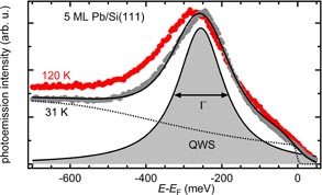
Figure 1. Laser photoemission spectrum in normal emission geometry (at
 ) for a 5 ML thick lead film on Si(1 1 1) for two different temperatures as indicated. The filled area represents the highest occupied QWS contribution to the spectrum, the dashed line represents the considered background including the Fermi–Dirac distribution function. The limited spectral resolution results in a finite spectral weight above the Fermi level. For a representative full band structure see figure 4.
Download figure:
Standard image High-resolution imageTemperature-dependent experiments were performed in several subsequent heating and cooling cycles by controlling the liquid Helium flow through the cryostat. Typical heating/cooling rates were < ±3.5 Kmin−1, resulting in relative errors of the temperature of <4% in a single photoemission spectrum at nominally fixed temperature. Figure 2 shows the temperature-dependent line width in two consecutive heating and cooling cycles. The line width gradually increases with sample temperature in the heating cycle and subsequently decreases upon recooling with almost the same gradient (0.36 meVK−1). A comparable response was observed for all film thicknesses under investigation in our experiments.
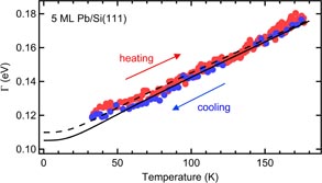
Figure 2. Temperature dependent photoemission line width of the highest occupied QWS in a 5 ML Pb/Si(1 1 1) film in the heating and cooling cycle (red and blue arrows, respectively).The dashed and solid line show the numerical solution of equations (2)–(4) for the heating and the cooling cycle, respectively.
Download figure:
Standard image High-resolution imageThe measured photoemission linewidth Γ can be decomposed by means of electron–electron (e–e), electron–phonon (e–ph) and electron–defect (e–df) contributions [34, 35, 38]:

It is generally expected that the photoemission line width contributions from e–ph and e–e scattering increase monotonically with temperature, while the electron–defect scattering contribution is temperature-independent. It should be noted that this is only true for sufficiently low defect densities as scattering from vibrating defects was previously shown to also exhibit a temperature dependence [36, 37]. In addition, defects might be thermally activated, leading to further temperature dependent contributions [39]. Since the electronic states under investigation here are energetically located in the vicinity of the Fermi level, e–e contribution to the photoemission line width plays only a minor role because of phase-space restrictions for e–e scattering events. Following the femtosecond time-resolved experiments by Kirchmann et al [16], e–e scattering limited lifetimes of carriers at these binding energies are in the range of τe−e ≈ 120–150 fs, resulting in a linewidth-contribution of
 . No significant temperature dependence of this contribution can be expected for temperatures well below the Fermi temperature [41]. The e–e scattering line width contributions for the states under investigation here are listed in table 1. Therefore, e–ph scattering dominates the line width broadening for electronic states in the vicinity of the Fermi level. The scattering rates can be expressed as:
where E denotes the electron binding energy (referenced to the Fermi level), α2F is the Eliashberg spectral function, f is the Fermi–Dirac distribution function and n is the Bose–Einstein distribution function [42]. Equation (3) accounts for all possible e–ph scattering events with energy transfer up to ±ℏωm, where ωm is the highest phonon frequency. The index
 indicates momentum-dependent quantities.
Table 1. Summary of the data obtained from the photoemission line width analysis. The e–e scattering contributions Γe−e were calculated within the framework of Fermi-liquid theory following reference [16]. EB and Γe−df denote the binding energy and the e–df contribution, respectively. EPC parameters
 were averaged over two heating/cooling cycles.
| Θ (ML) | EB (meV) | Γe−e (meV) | Γe−df (meV) |
 |
|---|---|---|---|---|
| 5 | 250 ± 5 | 1.9 | 108 ± 6 | 0.83 ± 0.09 |
| 7 | 155 ± 5 | 0.7 | 115 ± 8 | 0.76 ± 0.15 |
| 12 | 220 ± 4 | 1.5 | 93 ± 20 | 0.97 ± 0.48 |
Assuming a phonon-mode independent coupling strength
 of an electron with binding energy
 , the Eliashberg spectral function is reduced to the weightened phonon density of states [38] and can be approximated within the Debye model:

where ℏωD = 9.05 meV denotes the Debye-frequency of lead. Note that we have chosen the notation in a way that λ now refers to a specific electronic state and that this Eliashberg function differs from the well-known notation for all electronic states at the Fermi-level (see, e.g. [40]). In the high-temperature limit, equations (3) and (4) predict a linear increase in photoemission line-width with temperature, where the slope is determined by the EPC strength λ. In the limiting case T → 0, the line width is given by e–e and e–df contributions which can be separated using the e–e contributions reported in [16].
Numerical solutions of equations (2)–(4) are shown as solid and dashed lines in figure 2. From a least mean square fit to the experimental data, we obtained λ = 0.72 ± 0.08 (0.70 ± 0.04) for the heating cycle and λ = 0.74 ± 0.12 (0.74 ± 0.10) for the cooling cycle (first and second cycle, respectively). Because the variations in the different cycles are within the experimental uncertainty, we will discuss the averaged value
in the following. Table 1 summarizes the result of our measurements for different Pb film thicknesses.
The values for
 obtained here differ clearly from the values reported in literature for bulk lead (λ = 1.1–1.7) that mostly rely on momentum-averaging techniques [4]. To understand the origin of this significant difference we carried out DFT calculations, which are presented in the next section.
3.2. Density functional theory calculations
We performed density-functional perturbation theory calculations within the mixed-basis pseudopotential approach [43, 44] and the local density approximation for the exchange-correlation function. The scheme employs a combination of local functions and plane waves for valence states [43]. For plane waves, a kinetic energy cutoff of 20 Ry was used. Brillouin zone integrations were performed by sampling a uniform 48 × 48 × 1
-point mesh corresponding to 217 special points in the irreducible part of 2D Brillouin zone and a Gaussian energy smearing scheme with a width of 0.2 eV. To calculate dynamical and EPC properties, the linear response technique [45] is used. Details of the calculation as well as the spin–orbit coupling implementation within the mixed-basis pseudopotential method can be found in [46].
The calculations were performed both for free-standing Pb films and for the films with atoms at one side kept fixed to assume a rigid substrate. The momentum-dependent strength of e–ph interaction [47] is defined as:

When
is averaged over electron momentum at E = EF one obtains λ(EF), the averaged strength of e–ph interaction [48] at the Fermi level. λ(EF) evaluated for Pb(1 1 1) films with thicknesses ranging from four to 10 layers is shown in figure 3. All data were obtained with spin–orbit interaction included.
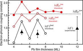
Figure 3. Electron–phonon coupling parameter λ(EF) averaged over electron momentum at the Fermi level as a function of Pb film thickness. The full and open red circles correspond to the calculations of free-standing films and the films with atoms at one side kept fixed, respectively.
for the highest occupied QWS are shown for the case of one film's side fixed (open black circles). All data were obtained with spin–orbit interaction included. Also shown are the experimental values (triangles). Note that the data for the momentum-averaged coupling strength of free standing films λ(EF)free have been published previously in [24].
Download figure:
Standard image High-resolution imageThe structure of films does not strongly modify the EPC. As shown in figure 3, both sets of λ(EF)free/fixed converge gradually to the calculated bulk parameter λ(EF)bulk = 1.56 [46] with increasing film thickness, which agrees with the experimental value of 1.55 [49]. Both for free-standing Pb(1 1 1) films and for the films with one side kept fixed the difference in the strength of e–ph interaction between the film and bulk values of λ(EF) is small and decreases quickly with film thickness. It should be noted that this is true only when the calculation includes spin–orbit coupling. Otherwise, the calculated strength of electron–phonon interaction is strongly underestimated [24, 46].
Figure 3 also shows the calculated
for the highest occupied QWSs (open black circles) that can be directly compared to our experimental results (triangles). The momentum-dependent e–ph coupling strength is largely determined by the QWS binding energy. For odd-layer films considered, the binding energy of the highest occupied QWS is small and therefore
is close to the strength of e–ph interaction at EF of the corresponding Pb(1 1 1) film. The calculated values of
for five- and seven-layer films linked to a rigid substrate are larger than the e–ph coupling strength obtained experimentally for QWSs in ultrathin Pb(1 1 1) films grown on a Si(1 1 1) substrate. Nevertheless, the assumption of a rigidly strained film results in lower values of λ, indicating the influence of the substrate on EPC strength in the thin film and the trend towards the experimentally obtained values. We thus conclude that changes of the films lattice constant along growth direction indeed modify the EPC strength in this system (as proposed earlier by Zhang et al [29]), but is not fully responsible for the large reduction with respect to the momentum-averaged bulk value.
3.3. Discussion
The discrepancy between the theoretical and experimental values for
can be attributed to the effect of the underlying Si substrate on the crystal and electronic structure of Pb overlayers, an effect not included in the calculation of the free-standing films. A simple assumption of a rigid substrate does not enable us to reproduce the strength of electron–phonon coupling in ultrathin Pb(1 1 1) films on Si(1 1 1) in agreement with the experimental data. To take into account the influence of Si(1 1 1) on both the crystal and electronic structure of Pb overlayers, one should consider a combined film-substrate system instead of treating the Pb(1 1 1) film as an independent quantum well system. Since the lattices of Pb and Si are incommensurate, it is an extremely difficult task to evaluate the electron–phonon interaction in such complex systems within ab initio approaches.
The effect of the silicon substrate on the electronic structure of Pb films has been demonstrated in many experimental studies [29, 50, 51]. It was shown that the Si substrate becomes an integral part of the Pb/Si(1 1 1) quantum system which can affect the details of electronic structure near the Fermi level and the electronic transport properties due to the incommensurate scattering at the interface [50] and the superconductivity of ultrathin Pb films.
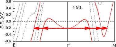
A possible scenario could be given by a change of the orbital character of the QWS induced by the presence of the substrate. The QWSs at
are of pz symmetry and an analysis of individual contributions to
from particular electronic states shows that the contributions from electronic states of pz symmetry dominate (see figure 4). The scattering to electronic states of in-plane (px, py) symmetry turns out to be negligible due to the different orbital character of initial and final states. So two main scattering channels for EPC are: (1) intraband scattering and (2) interband scattering into final states of pz character at large in-plane electron momenta. The contribution from both channels comes up to 70% of the
value. A change of the electronic states including symmetry (acquiring a partial px, py character) induced by underlying Si(1 1 1) substrate could reduce the strength of interband scattering and, thus, lower electron–phonon interaction. Further effects could contribute from substrate induced changes of the vibrational properties, which are, however, out of the scope of the present study.
Figure 4. Electronic band structure of a five-layer Pb(1 1 1) film along high-symmetry directions of the film Brillouin zone. The solid lines represent the bands of predominantly pz symmetry (at least near the QWS energy). Arrows indicate those electronic transitions which predominantly contribute to
.
Download figure:
Standard image High-resolution image
4. Conclusion
The electron–phonon coupling constants of thin Pb films on a Si(1 1 1) surface were measured for different film thicknesses and directly compared to DFT calculations on free standing and rigidly strained films. Significant differences can be found for Pb layers as thick as 12 ML that must be attributed to modifications of the Pb electronic and vibrational properties by the presence of the Si(1 1 1) substrate. No considerable confinement effects were found as the thin film value of λ rapidly converges towards the well-known bulk value with increasing film thickness. It must be concluded that this particular configuration must be treated as a combined film-substrate system. A similar behavior can be expected in other nanostructured materials that couple to a macroscopic environment.
Acknowledgments
The authors wish to thank M Tringides and U Starke for fruitful discussions. Financial support by the Deutsche Forschungsgemeinschaft through SFB 616, BO-1823/2 and FOR 1700 is gratefully acknowledged. We also acknowledge partial support from the Basque Country Government, Departamento de Educación, Universidades e Investigación (Grant No. IT-366-07), and the Spanish Ministerio de Ciencia e Innovación (Grant No. FIS2010-19609-C02-00), and 00), and the Ministry of Education and Science of Russian Federation (Grant No. 2.8575.2013).
Footnotes
- 7
Note that Θ represents the mass equivalent coverage which varies continuously between integer numbers of ML along the wedge.