
Abstract
The electronic structure of GaAs, InAs and InSb nanowires is studied using the six-band and the eight-band k⋅p models. The effect of the different Luttinger-like parameters (in the eight-band model) on the hole band structure is investigated. Although GaAs nanostructures are often treated within a six-band model because of the large bandgap, it is shown that an eight-band model is necessary for a correct description of its hole spectrum. The camel-back structure usually found in the six-band model is not always present in the eight-band model. This camel-back structure depends on the interaction between light and heavy holes, especially the ones with opposite spin. The latter effect is less pronounced in an eight-band model, but could be very sensitive to the Kane inter-band energy (EP) value.
Export citation and abstract BibTeX RIS
1. Introduction
Nanotechnology has evolved at a very rapid pace in the last decades. Several techniques, such as molecular beam epitaxy (MBE) [1] and the vapour–liquid–solid technique (VLS) [2], have been developed to realize nanostructures of various dimensions. The one-dimensional nanostructures known as nanowires exhibit some interesting properties such as a high dielectric constant which has already been realized in applications such as nanolasing devices [3]. The one-dimensional quantum confinement of nanowires has enhanced their transport properties. Nano-LEDs [4] and photovoltaic devices [5] have recently been experimentally realized. Semiconducting nanowires have also been used in building nanodevices such as sensors, photodetectors [6] and field effect transistors [7]. Theoretical backing and understanding of the basic physical properties of these emerging technologies has therefore become very essential.
Several methods have been used to describe the electronic properties of semiconductor nanowires such as density functional theory [8], tight binding [9, 10], pseudo-potential and the k⋅p method. Of all these, the k⋅p method is computationally the least expensive. It can accurately describe the band structure near the Γ-point. The Luttinger–Kohn k⋅p method has been successfully used to describe both zinc blende [11–13] and wurtzite crystal structures. It has been used to describe bulk structures for different growth directions and several potentials, such as strain [14, 15] and magnetic field, can be easily included into the Hamiltonian using this method. Different k⋅p models have been developed, depending on the number of bands that are included, see figure 1(a): a 4 × 4 Hamiltonian if only the Γ8 band (light hole (LH) and heavy hole (HH)) are included, a 6 × 6 model where also the Γ7 band (split-off (SO)) band is included and an 8 × 8 Hamiltonian when the Γ6 conduction band is also included. In all these models, phenomenological—Luttinger—parameters related to the effective mass of the charge carriers are needed. Furthermore, different expressions on how the Luttinger-like parameters for an eight-band model can be derived from the Luttinger parameters for a six-band model are given in the literature [16–18]. By applying the multiband effective mass approximations these bulk k⋅p Hamiltonians are used to describe the electronic structure of nanostructures.
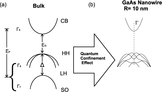
Figure 1. (a) Eight-band model for the III–V compounds studied in this paper, with conduction band (CB) Γ6 and the valence bands (HH, LH and SO), i.e. Γ8 and Γ7, where EG is the bandgap, Δ is the split-off energy and EP is Kane's energy. (b) Due to quantum confinement effects, the band structure of the nanowire includes mixing of the heavy-hole (HH), light-hole (LH) and split-off (SO) states, resulting in new features such as the camel-back feature.
Download figure:
Standard imageThe electronic properties of freestanding nanowires [19] made of various materials have been studied. In some of these materials the top valence band exhibits a camel-back structure even in direct bandgap semiconductors [20, 21]. This camel-back structure is due to the HH and LH mixing which is enhanced in nanostructures due to confinement, as also shown in figure 1(b). It results in a peak in the absorption spectrum and an increase in the exciton lifetimes. It has been proposed that tensile-strained multiple quantum-well (MQW) structures with a camel-back-shaped first valence subband can exhibit large refractive index changes due to current injection [22]. Properties due to the camel-back structure of the valence band in freestanding core–shell nanowires have been studied recently using multiband k⋅p models [20, 21]. It was found that the presence or absence of a camel-back depends on the k⋅p model (four- or six-band) and this was even more so for thinner wires. However, this study was only applicable for large bandgap materials, as four- and six-band models fail to describe materials with bandgaps much smaller than 1 eV, where the influence of the conduction band is large. This motivated us to apply in the present paper the six-band and eight-band k⋅p models to zinc blende freestanding nanowires with different bandgap values and compare the results for the hole states. We also focus on the camel-back structure as it is a particular feature of these nanowires. Furthermore, the effect of the different Luttinger-like parameters in the eight-band model on the hole electronic structure is investigated. We employed both the Pidgeon–Brown [16] and Bahder–Pryor [17, 18] approaches when modifying the Luttinger parameters. The effects of the choice of the Luttinger parameters is illustrated for the case of bulk semiconductors, where we choose GaAs as an example of a large bandgap semiconductor, and InAs and GaSb, which are low bandgap semiconductors. The choice of the appropriate set of the modified Luttinger parameters is an important issue in the case of nanostructures. In addition to bulk-related terms in the Hamiltonian which determine the expectation value of the kinetic energy, the electron and hole eigenenergies depend on the confinement potential. In freestanding nanowires, confinement breaks the condition of transversal symmetry, which leads to splitting of the energy levels. Furthermore, the boundary conditions for the electron and hole wavefunction are such that both the electron and hole are localized. Therefore mixing between them increases, which may lead to interesting effects in the band structure, like anti-crossings between the hole levels and a negative effective mass of the hole ground state (camel-back structure). When the bandgap is small, the effects of band mixing could also be large in the valence band and therefore application of the eight-band k⋅p approach is required, especially for low-bandgap semiconductors, like InAs and InSb. We analyse differences between the hole states obtained by using different Luttinger parameters. Furthermore, we analyse how the choice of the Kane parameter, which describes the coupling between the conduction (Γ6) and valence (Γ8 and Γ7) bands, affects the electronic structure. Our aim is to resolve whether important details are found in the eight-band model which are, however, missing in the six-band approach. We especially consider the conditions under which the camel-back features which are present in the ground valence subband according to six-band calculations, as previously found in [20, 21], are removed in the eight-band model. In order to resolve how different terms of the multiband Hamiltonian affect the hole dispersion relations, we compute the expectation values of a few dominant matrix elements in the multiband Hamiltonians. Special emphasis is put in a comparison of the contributions, of the diagonal terms and the terms that mix the heavy- and light-hole states of the hole subband to the energy.
2. Theory
Luttinger introduced the so-called Luttinger parameters γ1,γ2,γ3 to describe the Γ8 band in a 4 × 4 Hamiltonian H4. Later, not only the H4 Hamiltonian but also the 6 × 6 Hamiltonian was written with the same γj's. However, strictly speaking, the parameters that describe the Γ7 band in the H6 Hamiltonian, say γΔj, are equal to γj only for zero spin–orbit splitting. Boujdaria et al [23] showed that, to describe the bulk band structure of GaAs, γΔj ≈ γj is a good approximation, while for InAs, for example, γΔ1 is 74% smaller than γ1 and for InSb γ1 is almost four times larger than γΔ1.
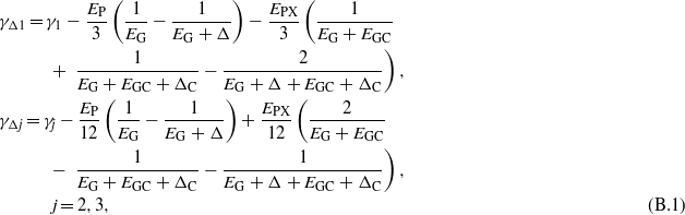
In order to describe simultaneously the conduction band Γ6 and the valence bands Γ8 and Γ7 in an 8 × 8 Hamiltonian H8 one has to introduce the Luttinger-like parameters  as a correction to the Luttinger parameters. This modification is a result of the Löwdin perturbation which should be employed when the eight-band model is modified to the six-band k⋅p theory. The essential parameter in this procedure is the energy of the unperturbed states, whose value depends on the range of energies of interest. In the literature, in essence, two sets of relations can be found. Pidgeon and Brown [16] used the following relations:
which were used both for the Γ8 and Γ7 bands. We will refer to these parameters as PB parameters. In papers by Bahder [17] and Pryor [18], the following relations were used:
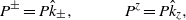
where the energy EG + Δ/3 is the difference between the energy of the conduction band and the energy of the centre of gravity of the valence band, as stated in [23] and will be referred to as BP parameters. Here EG is the bandgap, Δ is the split-off energy and EP is the Kane energy defined as

where  are the inter-band matrix elements between the conduction band (Γ6) and the valence bands (Γ8 and Γ7).
These different relations lead to large differences in the values for the  's as was shown in [23]: the ratio
  for GaAs is 1.19, for InAs 2.45, and for InSb even 16.06. However, it was convincingly shown in [23] that the correct expressions are the PB parameters.
Table 1. Band parameters, and Luttinger and Luttinger-like parameters for GaAs, InAs and InSb.
| GaAs [25] | InAs [25] | InSb [26] | |
|---|---|---|---|
| EG (eV) | 1.519 | 0.417 | 0.25 |
| EP (eV) | 23.81 | 21.5 | 24.08 |
| Δ (eV) | 0.341 | 0.39 | 0.82 |
| γ1 | 7.05 | 20 | 34.8 |
| γ2 | 2.35 | 8.5 | 15.5 |
| γ3 | 3 | 9.2 | 16.5 |

|
1.8251 | 2.8137 | 2.6933 |

|
−0.2625 | −0.0931 | −0.5533 |

|
0.3875 | 0.6069 | 0.4467 |

|
2.1888 | 6.8982 | 19.4624 |

|
−0.2411 | 1.9491 | 7.8312 |

|
0.5694 | 2.6491 | 8.8312 |
| γΔ1 | 5.8967 | 11.2505 | 9.603 |
| γΔ2 | 2.1516 | 6.4953 | 9.4425 |
| γΔ3 | 2.7194 | 7.0519 | 10.2549 |

|
1.6297 | 2.3699 | 2.1014 |

|
−0.2214 | 0.011 | −0.4199 |

|
0.3465 | 0.5027 | 0.3132 |
In section 3, we investigate the influence of the different relations, PB and BP, on the energy structure of a nanowire. We also address the question under what conditions a six-band model is sufficient and when an eight-band model has to be used and we investigate the effect of the approximations γj ≈ γΔj and  for a nanowire. Thus, where in [23] the bulk band structure was considered, here we focus on the influence on the energy structure of a nanowire with a special emphasis on the camel-back structure.
3. Bulk band structure
In this paper we concentrate on three zinc blende III–V semiconductors: GaAs, InAs and InSb. The Luttinger, Luttinger-like parameters, bandgap EG and spin–orbit splitting Δ used for those materials are summarized in table 1. For GaAs EG ≫ Δ, for InAs EG ≈ Δ, and for InSb EG ≪ Δ. Before discussing the effects of the different relations, PB and BP, on the electronic structure of the nanowire, we first show the bulk valence band structure for these three semiconductors in figure 2 given by H6 (with the Luttinger parameters) and H8 (both with the Luttinger-like parameters from the relations PB and BP). Here the approximations γj ≈ γΔj and  were made. Thus only three Luttinger and Luttinger-like parameters were used. The bulk band structure is calculated for the different directions [001], [110] and [111]. In the appendix the explicit expression of the Hamiltonian used is given.
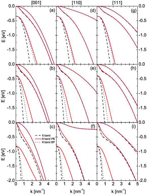
Figure 2. Bulk band diagrams for ((a), (d), (g)) GaAs, ((b), (e), (h)) InAs and ((c), (f), (i)) InSb along the [001], [110] and [111] directions. Results are shown for six-band (dashed lines), eight-band using PB parameters (solid lines) and eight-band using BP parameters (dotted lines).
Download figure:
Standard imageFrom figure 2 we see that for bulk GaAs we can see that the H6 Hamiltonian is sufficient to describe the bulk valence band structure. The results obtained with the H8 model with both sets of Luttinger-like parameters are also very similar, because EG ≫ Δ. For bulk InAs, the light-hole band obtained from H6 starts to deviate from the most accurate result obtained with H8 and the Luttinger-like parameters PB. This deviation is even more pronounced for InSb. Note that the light-hole band obtained with H8 and the Luttinger-like parameters BP is almost identical to the one obtained with H6. This shows that the Luttinger-like parameters BP underestimate the coupling between conduction and valence bands. So we can conclude that, to describe the bulk band structure, the six-band model (H6) works well for GaAs, but for InAs and InSb one should use the eight-band model (H8). In section 4 we investigate whether the same conclusions are valid for freestanding nanowires made of these materials.
4. Band structure of nanowires
Let us now investigate if the same models also describe correctly the valence band structure of a nanowire. As we are interested in the effects of band mixing due to the confinement effect, we consider thin GaAs, InAs and InSb cylindrical nanowires grown in the [001] crystallographic direction with a radius of 10 nm. This choice of radius R = 10 nm is made to properly illustrate the camel-back feature of the top valence band. Figure 3 shows the energy difference between the ground state energy and the first four excited states at Γ as a function of the radius. The energy difference between the ground and the excited states decreases as we increase the radius of the wire, thus making R = 10 nm the ideal choice where the camel-back feature might be prominent. Furthermore, nanowires with such diameters have already been synthesized [24]. The valence band structures obtained with the same three Hamiltonians are shown in figure 4. As stated in [23], the PB relations (equation (1)) are the most accurate Luttinger-like parameters. Therefore we consider the solid curves in figure 4 as the most accurate ones.
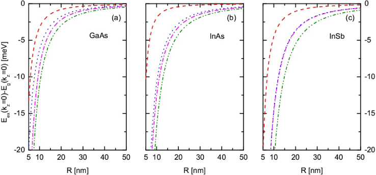
Figure 3. Energies of the first four excited states with reference to the ground state energy at kz = 0 for different radii (R = 5–50 nm) using PB relations (equation (1)) for GaAs (a), InAs (b) and InSb (c) nanowires, respectively.
Download figure:
Standard image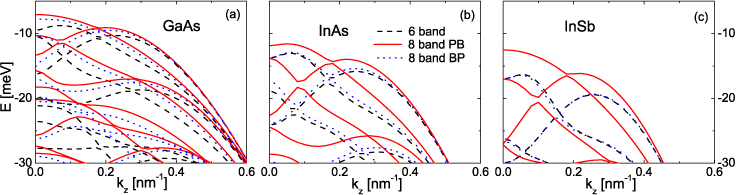
Figure 4. Valence subbands of (a) GaAs, (b) InAs and (c) InSb nanowires with radius R = 10 nm grown in the [001] direction obtained using three different models.
Download figure:
Standard imageFrom the previous bulk results on GaAs it is expected that for small k values the six-band model is sufficient to describe the valence band electronic structure. However, note that in figure 4(a) a camel-back structure is observed in the top of the valence band in the six-band model, while it is absent in both eight-band models. This shows that, although GaAs nanostructures are often treated in the literature within a six-band model, an eight-band model might be necessary for a correct description of the valence band structure. The general idea that the size of the bandgap with respect to the spin–orbit splitting [23] is the crucial factor that determines if a six-band model is sufficient, or that an eight-band model is necessary, is thus not correct. The reason is that the value of EP is another important factor. EP couples the conduction band Γ6 with the valence bands Γ7,Γ8 and is proportional to the square of the matrix element 〈S|px|X〉, which is independent of the bandgap EG.
Let us now consider the case of an InAs nanowire as shown in figure 4(b). Because EG ≈ Δ, it is expected that an eight-band model is necessary to describe the electronic structure correctly. Here, the six-band model shows a camel-back structure, but it also appears in both eight-band models (see figure 4(b)). However, in the case of InSb nanowires there is no camel-back structure in the eight-band using PB relations (equation (1)), but there is one in the other two cases. For both InAs and InSb nanowires, the six-band model is not accurate, as can be expected from their small gap values in comparison with the spin–orbit splitting. But also note that the eight-band model with the Luttinger-like parameters BP differs significantly from the eight-band model with the correct Luttinger-like parameters PB. The results of the former eight-band model coincides almost with the results from the six-band model, showing again an underestimation of the coupling between valence and conduction bands. Thus, we will use the Luttinger-like parameters PB in the rest of the paper. Also it is important to note that the camel-back structure observed in the six-band results is not always present in the eight-band model (see figure 4). Therefore we explore the properties of the camel-back structure further in section 5.
But first we illustrate the effect of the approximations γj ≈ γΔj and  on the nanowire valence band. As stated in [23], for large EG or small Δ, the approximations γj ≈ γΔj and
  are valid. Figure 5 shows the valence band structure again for the same GaAs, InAs and InSb nanowires, obtained within the eight-band model with both the three-parameter (eight-band PB3) and the six-parameter (eight-band PB6) model. From these results it is very clear that the approximations γj ≈ γΔj and
  are valid for GaAs nanowires. In the case of InAs and InSb there are some small differences for the excited hole states but still the approximation appears to be reasonably accurate. Thus we will make the approximation γj ≈ γΔj and
  in the rest of the paper.

Figure 5. Valence subbands of (a) GaAs, (b) InAs and (c) InSb nanowires with radius R = 10 nm as obtained using the three-parameter (solid curves) and the six-parameter (dashed curves) models.
Download figure:
Standard image5. Camel-back structure and its properties
The camel-back structure which was observed in the ground state valence subband dispersion relation is a very interesting feature as the effective mass in this region is negative, which is opposite to the bulk effective mass of the holes. This results in an increase in the number of equal energy transitions between the ground state valence band and the conduction bands. In [20, 21], the authors have studied the camel-back structure in both freestanding nanowires and core–shell nanowires. They have shown that this camel-back structure can result in a peak in the absorption spectra which should be experimentally observable. In the present paper we discuss the properties of the camel-back structure in freestanding nanowires using an eight-band k⋅p model.
Let us now discuss the camel-back structure in more detail. In figure 4 it is very clear that, except for InAs, the camel-back structure is only seen in the six-band model. However, different EP values can be found in the literature for InAs, EP = 21.5 eV in [26] and EP = 22.2 eV in [27]. In order to show the importance of EP, figure 6(b) gives the valence band structure for the same InAs nanowire, where the valence band structures for both values are given. Here EP = 21.5 eV [26] gives a small camel-back as mentioned before, but a slightly larger value of 22.2 eV [27] removes this effect. We do a similar study for the GaAs nanowire (see figure 6(a)), where we use EP = 15 eV (unrealistic value) and EP = 23.81 eV [25] for the eight-band model, which confirms that a smaller value of EP gives results closer to the six-band model. Also similar results are obtained for the InSb nanowire using different EP values, EP = 23.3 eV [26] and EP = 24.08 eV [25] (see figure 6(c)). Note that, in the case of GaAs, a value of EP = 21 eV which is obtained from the theoretical relation [28]

which is often suggested to remove spurious solutions, also produces a small camel-back. This shows clearly that the band structure is very sensitive to the EP value.

Figure 6. Valence subbands of (a) GaAs, (b) InAs and (c) InSb nanowires with radius R = 10 nm obtained using the PB parameters with different EP values.
Download figure:
Standard image
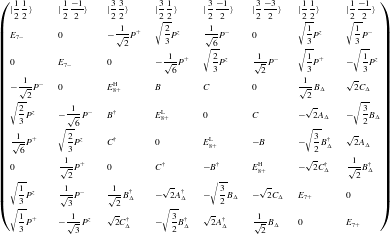
As figure 6 shows, the camel-back feature occurs if the six-band model is adopted and is missing in the eight-band model for large EP values. In order to get more insight into the existence of the camel-back structure, we resolve the contributions of the Hamiltonian matrix elements to the hole ground subband energy. If we denote the normalized ground state wavefunction in the eight-band model by  , where
  (x
(x {e,hh,lh,so}) are the envelope wavefunctions corresponding to the Bloch function |jm〉, the energy of the ground state is expressed as the sum of the expectation values of its matrix elements:
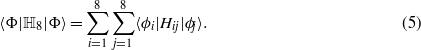
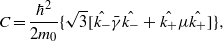
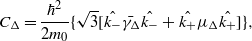
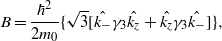
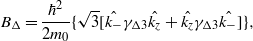
We note that, because of the symmetry of the confining potential, the hole subbands in a nanowire are double Kramers-degenerate. Furthermore, because of the Hermitian character of the Hamiltonian, the expectation values of the matrix elements Hij and Hji are complex conjugates of each other. Therefore their joint contribution to the valence subband energy amounts to 2Re(〈ϕi|Hij|ϕj〉). As a matter of fact, the valence band energy can be resolved in the following contributions of the zone-centre states: (1) the electron zone-centre states EL = 〈ϕ1|H11|ϕ1〉 + 〈ϕ2|H22|ϕ2〉, (2) the heavy-hole zone-centre states HH = 〈ϕ3|H33|ϕ3〉 + 〈ϕ6|H66|ϕ6〉, (3) the light-hole zone-centre states LH = 〈ϕ4|H44|ϕ4〉 + 〈ϕ5|H55|ϕ5〉, (4) the split-off zone-centre states SO = 〈ϕ7|H77|ϕ7〉 + 〈ϕ8|H88|ϕ8〉, (5) the mixing term B between the heavy and light holes B = 2Re(〈ϕ3|H34|ϕ4〉) and (6) the contribution of the mixing term C between the light and heavy holes C = 2Re(〈ϕ3|H35|ϕ5〉). It turns out that the contribution of SO and the terms which mix the electron and hole zone-centre states (P terms, see the appendix) are much smaller than the ones due to mixing between the heavy- and light-hole zone-centre states. Therefore, we do not include them in our discussion below. The total energy of the hole (valence band) state is denoted by VB in all diagrams. The calculation is performed for nanowires made of the same three materials as before, which have a different ratio between the bandgap and the split-off energy: (1) GaAs, where EG ≫ Δ, (2) InAs, where EG ≈ Δ, and (3) InSb, where EG ≪ Δ. The results are given for nanowires with a radius R = 10 nm. Qualitatively, the same results were found for other radii.
5.1. GaAs nanowire (EG ≫ Δ)
In figure 7 we present the valence band ground state energy (VB) and the most important contributions to its energy for a GaAs nanowire of radius R = 10 nm. Results obtained by using three different models are shown: the six-band model which is shown in figure 7(a), the eight-band model with EP = 15 eV in figure 7(b) and EP = 23.81 eV in figure 7(c). The diagonal heavy-hole (HH) and light-hole (LH) contributions decrease as a function of kz. However, the contribution from the interaction between the heavy and light holes (B and C) increases in the six-band model, which appears to be the origin of the camel-back structure. In the results of the eight-band model (see figure 7(c)), this increase is much smaller, especially the contribution from the interaction between the heavy and light holes with opposite spin (C), which leads to the disappearance of the camel-back structure. This change in coupling between heavy and light holes can only be caused by the extra coupling of both bands with the conduction band, whose strength is given by the value of EP, which can be seen from the contributions in figure 7(b), where EP = 15 eV. In general, we see that the diagonal terms HH and LH increase with increasing EP. However, the coupling terms, B and C decrease with increasing EP. The different contributions in figure 7 show discontinuities which are due to the ground state transitions as a function of kz visible in the band diagram of figure 6.
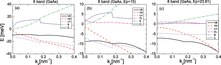
Figure 7. Valence ground state and important contributions to it, for a GaAs nanowire with radius R = 10 nm obtained using the PB parameters for (a) the six-band model, (b) the eight-band model with EP = 15 eV and (c) the eight-band model with EP = 23.81 eV.
Download figure:
Standard image5.2. InAs nanowire (EG ≈ Δ)
In the case of the InAs nanowire, we present results for two sets of EP values, EP = 22.2 and 21.5 eV for R = 10 nm (see figure 8). The diagonal terms HH and LH in the six-band model have a camel-back shape. But here we see that the coupling between light and heavy holes of opposite spin (C) decreases with kz for the six-band model, whereas this was opposite in the case of GaAs. In the case of the eight-band model the camel-back shape of HH and LH terms vanishes, but C behaves just as in the six-band GaAs case. The coupling term B is always increasing in both GaAs and InAs, since it is proportional to kz. Also it is worth noting that the energy of the heavy-hole (HH) term is not affected by changing the EP value (see figures 8(b) and (c)).
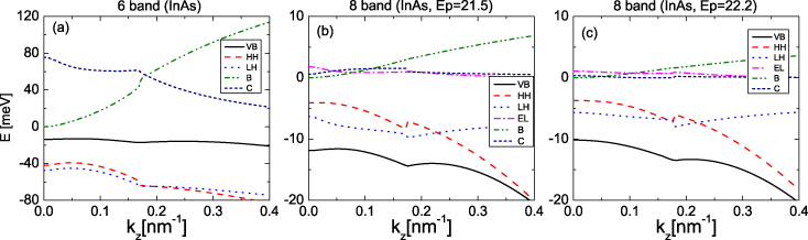
Figure 8. Valence ground state and important contributions to it, for a InAs nanowire with radius R = 10 nm obtained using the PB parameters for (a) the six-band model, (b) the eight-band model with EP = 21.5 eV and (c) the eight-band model with EP = 22.2 eV.
Download figure:
Standard image5.3. InSb nanowire (EG ≪ Δ)
Finally we look at the InSb nanowire results. Here we take two sets of EP values, EP = 24.08 and 23.3 for R = 10 nm (see figure 9). Here also the diagonal terms decrease with increasing kz, and the coupling terms B and C show similar behaviour as in the case of InAs. An increase in EP value decreases the contribution of the coupling terms B and C and thus reduces the camel-back feature.
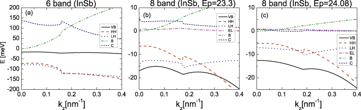
Figure 9. Valence ground state and important contributions to it, for an InSb nanowire with radius R = 10 nm radius obtained using the PB parameters for (a) the six-band model, (b) the eight-band model with EP = 23.3 eV and (c) the eight-band model with EP = 24.08 eV.
Download figure:
Standard image5.4. Discussion
From the above results it is evident that, in the case of wide-gap materials like GaAs, one needs a large change in the EP value in order to restore the camel-back structure in the eight-band model. This is not the case with small bandgap materials like InAs and InSb, where even a small change in the EP value brings back the camel-back in the eight-band model. These results are consistent with the PB relations (equation (1)), where we can see that the ratio EP/EG is an important factor. If we compare the Luttinger and the Luttinger-like parameters (see table 1), it becomes clear that the direct HH–LH coupling, through B and C, is overestimated in the six-band model. Comparison of the expected values of B and C in the six-band and the eight-band models leads to the same conclusion. Also it is important to note that, in the case of InAs  , which appears in the coupling term C (see the appendix) is large (≈0.5) when compared to the values for GaAs and InSb (≈0.1) (see table 1). This different value of
  is responsible for the smaller contribution of the C term which in turn is responsible for the presence of the camel-back in the InAs eight-band results (see figure 8). From the eight-band model results, which show a camel-back structure, i.e. in GaAs with EP = 15 eV (figure 7(b)), in InAs with EP = 21.5 eV (figure 8(b)) and in InSb with EP = 23.3 eV (figure 9(b)), it is clear that the camel-back feature for the ground state hole subband is observed only when the light-hole behaviour is opposite to the behaviour of the coupling term C.
6. Summary and conclusions
We have made a comparative study of the valence band structure as obtained within the six-band and the eight-band k⋅p models. Also we compared the results as obtained with different relations for the Luttinger-like parameters in the H8 Hamiltonian that can be found in the literature. We find that, in the case of nanowires, an eight-band description is necessary to obtain the correct valence band structure for GaAs, despite its large bandgap. This is due to the large EP value that gives the strength of the coupling between valence and conduction bands. For InAs and InSb nanowires, an eight-band model is also necessary for a more complete description of the valence band structure, as expected based on their small bandgap values. The Luttinger-like parameters presented in [17] underestimate the coupling between valence and conduction bands, and it is important to rely on the correct Luttinger-like parameters as given in [16] to describe the valence band structure of nanowires with a small bandgap. The camel-back structure which is observed in the six-band model for all the materials is not always observed in the case of the eight-band model. It can result in a peak in the absorption spectra as calculated in [20, 21] and also increase the exciton recombination lifetimes [29]. We found that the mixing between the light- and heavy-hole bands give the largest contribution to the camel-back structure. This mixing is overestimated in wires treated within the six-band model. These mixing terms are affected by variations of Kane's inter-band energy EP, in particular for narrow-gap materials. In conclusion, our theoretical results show that the possible presence of a camel-back structure in the hole ground subband dispersion is very sensitive to the choice of the EP value.
Acknowledgments
This work was supported by the Flemish Science Foundation (FWO-Vl), Belgian Science Policy (IAP) and the Ministry of Education and Science of Serbia.
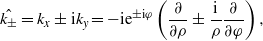
Appendix A.: Eight-band Hamiltonian
The Luttinger–Kohn (LK) Hamiltonian for an eight-band model [16, 17] is given by

where the terms with operators B and C give the interaction between the various valence band states of the same and the opposite spin, respectively, and terms with the P operator give the interaction between the valence and the conduction band states:
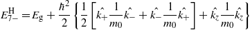
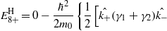
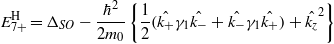
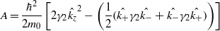

where


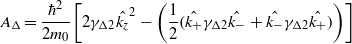
Appendix B.: Three-parameter and six-parameter models
In [23] the Luttinger and Luttinger-like parameters for the split-off band Γ7 (γΔi and  , respectively) are given and have the following form (EPX, EGC and ΔC are taken from [25])
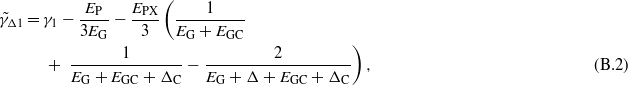
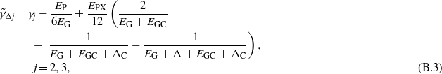
where EPX, EGC and ΔC are related to the higher conduction bands (Γ7C and Γ8C) (see figure 1 in [23]) and they account for the influence of the Γ7C and Γ8C bands on the split-off band Γ7.
The approximations γj ≈ γΔj and  give AΔ = A, BΔ = B and CΔ = C in the eight-band Hamiltonian H8.