

Abstract
Recently developed advanced scintillators, which have the ability to distinguish gamma-ray interaction events from those that accompany neutron impact, require improved quantum efficiency in the blue to near UV region of the spectrum. We utilize GaAs/Al0.8Ga0.2As photodiode elements as components in a wide band-gap solid-state photomultiplier as a lower-cost, lower logistical burden, and higher quantum efficiency replacement for the photomultiplier tube. An AlAs window layer is employed as a means to increase the diode's optical performance. Relative to structures absent the window layer, simulations and measurements demonstrate that the AlAs layer produces a spatial coincidence between regions of large drift fields with regions of high photon absorption. In addition to the AlAs layer, secondary ion mass spectrometry measurements show that an unexpected high degree of inter-diffusion of GaAs and AlAs quenches the photon-detection efficiency, a decrease that can be avoided by its post-growth removal. With the AlAs layer, the peak external quantum efficiency of 49% is achieved at 450 nm with 10 V reverse bias, which does not fully deplete the device. Simulations show that full depletion can result in efficiencies exceeding 90%. In order to enhance the optical response, a simple anti-reflective coating layer is designed using the existing passivation layer components that successfully minimizes the reflection at the wavelength range of interest (300 nm–500 nm).
Export citation and abstract BibTeX RIS
1. Introduction
For nuclear radiation sensing applications, scintillation materials remain competitive with higher energy-resolution semiconductor-based compounds because of the lower cost associated with their large-volume deployment. The current dominant photon sensor for scintillation photons, the photomultiplier tube (PMT), is bulky, fragile, sensitive to external magnetic fields, and has limited optical sensitivity, particular in the UV-blue wavelength range at which advanced scintillators, such as LaBr3 [1, 2], Cs2LiLaBr6 [3], and Cs2LiYCl6:Ce (CLYC) [4] operate. All of these deficiencies can be mitigated by solid-state technologies. Although silicon photomultipliers are already been developed and commercialized, they have poor UV sensitivity, and silicon's relatively low band-gap (1.1 eV) limits the area of a single two-terminal element to roughly 1 cm2 in order to avoid dark-count induced resolution loss [4].
Although AlGaAs/GaAs optical sensors and heterostructures are ubiquitous in the literature [8], we report on optical sensors based on the indirect and higher band-gap family AlAs/Al0.8Ga0.2As for the first time, a material combination that provides lower dark noise for single-photon detection applications compared with GaAs-based devices. Relative to the direct band-gap nitride-based devices, the greater penetration depths of the blue-UV photons targeted mitigates the effects of surface-induced charge trapping. In particular, this work is driven by the goal to replace the PMT used in radiation sensing applications by a lower-cost, more mechanically robust, higher performance solid-state alternative, particular for blue and near-UV photons emitted by emerging scintillation materials.
We previously demonstrated that Al0.8Ga0.2As diodes are responsive to the blue and near UV in both linear and breakdown modes [5, 9]. Furthermore, the PN and PIN junctions exhibit reproducible and low pre-breakdown leakage current as well as breakdown voltages that are insensitive to the diode shape, an invariability that demonstrates that the beveled edge design results in the confinement of the high electric field region to the central part of the diode [5, 9]. Surface proximate recombination, however, can reduce the quantum efficiency, particularly at shorter wavelengths due to the shallower penetration depths of the near UV photons. In order to mitigate the effects of surface-proximate trapping and recombination, an AlAs layer is introduced as a window through which short-wavelength photons can penetrate into the buried Al0.8Ga0.2As NP junction, because the absorption length associated with photons in the wavelength range of interest (300–500 nm) is nearly twice that of Al0.8Ga0.2As. In this paper, we focus on the optical effects of the AlAs layer when coupled to an Al0.8Ga0.2As photodiode.
2. Secondary ion mass spectroscopy (SIMS) of AlGaAs epi-layer structure
Metal-organic chemical vapor deposition epitaxial wafers were obtained from a commercial vendor given the layer structure illustrated in figure 1, which shows a GaAs/AlAs/AlGaAs layer structure on top of a p+ GaAs substrate. The total thickness of the epi-layers is approximately 1 m and the top n+ GaAs is included in order to improve the ohmicity of the contact between the metal electrode and the diode. As reverse bias voltage is applied, the depletion region is designed to grow upwards towards the surface from the interface between p-type and n-type Al0.8Ga0.2As. One of the advantages of utilizing a GaAs/AlAs/AlGaAs hetero-junction structure, compared with a III-nitride based device for instance, is the excellent lattice matching of the layers since the lattice constant of GaAs (5.65 Å at 300 K) deviates less than a picometer from that of AlAs (5.66 Å at 300 K) [10].
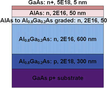
Figure 1. The designed vertical layer structure of the GaAs/AlGaAs photodiode element.
Download figure:
Standard image High-resolution imageIn order to realize the desired electrical and optical properties, it is important to determine the degree to which the grown epilayers match the design specifications, in terms of the doping concentrations, the mole fractions of both Al and Ga, and the thicknesses of the layers. Note that very low doping concentrations of less than 1 × 1016 cm−3 are difficult to achieve at present due to the presence of unintended, electrically active impurities. A SIMS analysis, shown in figure 2, illustrates that the realized wafers differ from the design as follows. First, at the GaAs/AlAs interface, an extended graded region exhibits a high Ga concentration because of species inter-diffusion. The transitional layer changing from GaAs to AlAs is observed to extend almost 20 nm into the wafer depth. Since AlxGa1−xAs with a low Al mole fraction (x < 0.3) has much higher optical absorption than AlAs, as shown in figure 3, most of the short wavelength photons are absorbed at the surface of the window where the graded region exists if it is not removed. This, in turn, decreases the photon detection efficiency because of the coincident between regions of highly probable absorption and high trapping.
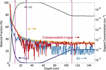
Figure 2. SIMS analysis results on the design structure illustrated in figure 1. The left ordinate shows the atomic fraction of Al and Ga within the arsenide matrix, and the right ordinate shows the doping concentrations of the n-type (Si) and p-type (Be) dopants. Purple colored lines indicate the depth to which the window is etched in three separate devices (A, B, and C). The disparate behavior between devices A and B shows the effect of the surface transitional layer, and a comparison between devices B and C indicates the effect of the AlAs layer [7]. (Reproduced with permission from [7], 2015 SPIE.)
Download figure:
Standard image High-resolution image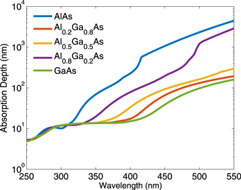
Figure 3. Variation in the absorption length as a function of wavelengths for AlAs, Al0.2Ga0.8As, Al0.5Ga0.5As, Al0.8Ga0.2As, and GaAs.
Download figure:
Standard image High-resolution imageThe lack of abruptness in the layer boundaries is also observed in the silicon (Si) n-type doping and the beryllium (Be) p-type doping of figure 2, noting that the beryllium is intended to compensate the Si in order to provide a region with low (<1017 cm−3) effective n-type doping over the depths shown.
3. AlGaAs photodiodes fabrication process
In fabricating the photodiodes, the diode area is first defined utilizing plasma-based dry-etching because the process delivers higher device yield compared with phosphoric acid wet-etching processes [6]. By controlling the gas proportion and the plasma power, as detailed in [6], beveled sidewall features were realized which mitigates the concentration of electric field at the sidewalls. Once the diode area is defined, the top GaAs layer is removed at the window area in order to minimize absorption in that thin highly doped layer used to realize an effective ohmic junction. The main result described below is the optical effect that results from window etching through either: (1) the GaAs layer alone (10 nm etch), (2) the graded layer transitioning from GaAs to AlAs (30 nm window), or (3) the AlAs layer as well as the graded layers (etching through a depth of 120 nm).
For the window area etching, citric acid (C6H8O7) and hydrogen peroxide (H2O2) with a ratio of 4:1 solution is used for selective GaAs layer etching. However, the complete GaAs/AlAs graded layer which extends to a depth of 20 nm cannot be removed with the citric acid solution due to high selectivity between GaAs and AlGaAs, noting that the 4:1 citric acid solution has a selectivity of 97.2 for GaAs over Al0.3Ga0.7As [5]. The utilization of the citric acid etching results instead to an etch depth of 10 nm (±2 nm). The remaining Al0.8Ga0.2As transition layer limits the absorption of incident photons within the desired active region where the electric field is developed. In order to remove the entire graded layer up to 30 nm, non-selective dry etching with combination of BCl3, Cl2, and Ar gas is adopted (see [5]). The resulting etch depth was 32 nm (±2 nm), which is confirmed with a Dektak 6 m surface profiler.
The beveled sidewall can act as a current leakage path and a source of surface recombination. In order to mitigate both deleterious effects, sulfur is utilized to tie-off the dangling bonds, and a silicon nitride layer prevents oxidation and contamination after the processing. The nitride layer is not only a passivation layer but also functions as an anti-reflective coating (ARC). For the ARC, we aimed to minimize the reflectance in the wavelength range of 300 nm–500 nm, with a minimum at 380 nm, the peak wavelength of CLYC [4].
Following the passivation steps, the fabrication is finalized with two evaporated metallic depositions to make ohmic contact upon the top-side n+ GaAs (50 nm Ni/325 nm Ge/650 nm Au/200 nm Ti/550 nm Au ) and the p-type GaAs (50 nm Pd/200 nm Zn/200 nm Pd/250 nm Au) substrate.
4. TCAD simulation
Sentaurus simulations, that utilize the experimental doping and concentration profile derived from the SIMS measurements, indicate that 40 nm of silicon nitride results in the lowest reflectance at the targeted range of the wavelengths, as illustrated in figure 4. Any small variation in the thickness of the nitride layer substantially alters the valley location of the reflectance curves; therefore, the thickness has to be carefully controlled during processing. Note in figure 4 that since the simulation result is based solely on the epitaxial structure without including the GaAs substrate, absorption decreases and the transmittance increases rapidly as the wavelength increases beyond 450 nm.
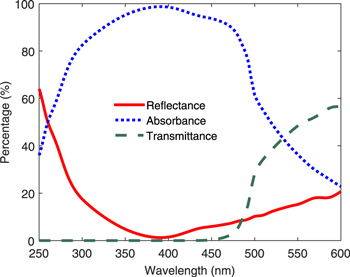
Figure 4. Reflectance, transmittance, and absorbance from the Al0.8Ga0.2As photodiode with a 40 nm thick silicon nitride anti-reflective coating layer.
Download figure:
Standard image High-resolution imageIn order to maximize the detection efficiency in a material with non-negligible charge trapping, the electric field should rapidly drift the photo-generated carriers to the collection electrodes. As shown in the Sentaurus TCAD electric field simulation of figure 5, which shows the electrical field development inside the devices with increasing bias voltage, the depletion initiates at the N/P Al0.8Ga0.2As interface and grows most rapidly into the n-type Al0.8Ga0.2As layer since the material has two orders of magnitude lower doping concentration than the p-type Al0.8Ga0.2As. As the bias voltage increases, the depletion region expands toward the surface, increasing the active absorption region particularly for short-wavelength photons, and is saturated at roughly 30 V. The topmost portion of the AlAs layer, at a depth of 20 nm from the surface, is more highly doped than Al0.8Ga0.2As layers, the effect of which is: (1) minimal penetration of the electric field into the highest part of the AlAs, and (2) a highly uniform electric potential across the bounding AlAs, which results in a uniform electric field across the diode area. A simulation, similar to that shown in figure 8, of the absorbed photon density as a function of depth, indicates that 30% of the incident photon flux at 430 nm is absorbed in the graded interface layer between GaAs and AlAs, and its removal is therefore necessary to realize high quantum efficiencies.
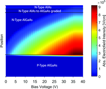
Figure 5. Variation in the electric field at the center of the circular diode, as the reverse bias voltage is varied.
Download figure:
Standard image High-resolution image5. Quantum efficiency comparison
Comparing the diodes with different recessed windows, figure 6(a) is the measured external quantum efficiency (EQE) from the structure that nominally has the GaAs layer removed (10 nm etch depth, slice A in figure 2), but in practice, retains a transitional AlAs layer that has a substantial Ga concentration. If one removes the Ga-graded transitional layer by etching down to 32 nm (slice B in figure 2), then figure 6(b) shows that the detector's photon detection efficiency increases by nearly four times.

Figure 6. External quantum efficiency (EQE) for the Al0.8Ga0.2As structure of figures 1 and 2 as a function of reverse bias for three different window etch depths: (a) 10 nm (slice A in figure 2), (b) 32 nm (slice B) and (c) 120 nm (slice C in figure 2). The EQE is measured with an Agilent Cary 5000 UV–vis–NIR photospectrometer acting as the light source and a picoammeter for the current measurement [7]. (Reproduced with permission from [7], 2015 SPIE.)
Download figure:
Standard image High-resolution imageThe main function of the AlAs layer is as a dark-noise reduction layer, in which the near-surface region is isolated from the active region by an intervening window that ideally would have zero photon absorption. As reflected in figure 3, the absorption can be quite low but it is non-negligible across the wavelength band of interest. The question is: if the AlAs layer is fully removed, does the loss of photon absorption in the AlAs layer-accompanied by carrier drift and diffusion into the depletion region-lower the EQE to a degree greater than the carrier loss associated with having a high surface recombination region within the Al0.8Ga0.2As np structure itself? As show in the experimental plots of figure 6(c), the presence of the AlAs layer improves the EQE.
The Sentaurus TCAD simulated EQE spectra of the two recessed window devices, shown in figure 7, demonstrate that the EQE is substantially increased-for partially depleted devices-when the AlAs layer is present, particularly for shorter wavelengths in the range of 300 nm–450 nm. Both of the devices exhibit a maximum EQE at roughly 470 nm at low bias, a peak that shifts towards 400 nm at high bias because of the expansion of the depletion region into those regions in which blue and near-UV photons have greater absorbance. Specifically, the absorbed photon density at 400 nm is displayed in figure 8. This figure shows the AlAs layer moves the position of maximum absorption probability deeper within the overall structure and more importantly, to a position where the electric field is non-negligible. Thus, the coincidence between the high electric field and the sizable absorption probability results in improved detector photon detection efficiency. Note that the sharp decrease of EQE at around 555 nm in figure 7(b) is due to the band edge of AlAs.
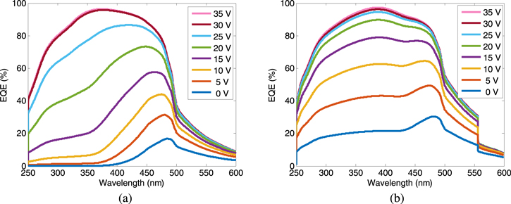
Figure 7. Simulated EQE results from the structure (a) without an AlAs layer [7] and (b) with an AlAs layer which functions as a semi-transparent window for shorter wavelength photons. This, in turn, enhance the efficiency by increasing the chance of collection inside the device. (Reproduced with permission from [7], 2015 SPIE.)
Download figure:
Standard image High-resolution image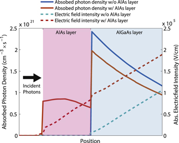
Figure 8. The absorbed photon density at a photon wavelength of 400 nm and the electric field in the devices both with and without the AlAs layer as a function of position. Without the AlAs layer, the position of highest photon absorption probability coincides with the low field region, both occurring near the surface. With the doped window layer, in contrast, the higher drift field, and expected lower trapping, at the position of maximum photon absorption results in greater quantum yield.
Download figure:
Standard image High-resolution image
In comparing the simulated EQE plots of figure 7 with the measured results in figure 6, both show a peak EQE location at ∼470 nm and an increase in efficiency with increased bias, noting that the since we assume perfect quantum yield in the device simulation, the simulated EQE results are ∼10%–20% higher. For instance, the peak EQE at 10 V is 64.5% for the simulated device with the AlAs layer (figure 7(b)), compared with a measured EQE of 48.9% (figure 6(b)). The device that has the AlAs layer removed (figure 6(c)) has maximum EQE of 23.6% at 10 V which is 25.3% less efficient than the device with the AlAs layer, but 10.2% more than the device with the photon-absorbing transitional layer.
The main behavioral discrepancy between the measured and simulated efficiency plots is the abrupt increase in experimental response between 5 V and 10 V, which is most likely due to the existence of an inversion layer in the compensated n-type doping between 20 nm and 60 nm, which retards the electric field growth until higher bias is applied, noting that even though the window is etched, the full GaAs/AlAs/Al0.8Ga0.2As structure exists under the electrodes. Furthermore, for the experimental diodes studied, the increase in dark noise above 15 V prevented an optical measurement at higher bias with our photospectrometer setup. As suggested in figure 7, the realization of a high EQE diode requires the application of reverse bias exceeding 35 V.
6. Conclusions
Through SIMS measurements of the doping and concentration profiles, we found a high Ga concentration transitional layer to the underlying device structure, the presence of which can critically deteriorate the device performance by absorbing incident broadband photons. The near-surface absorption is mitigated with a recessed window in which the EQE is improved from 13% to 49%, in a partially depleted diode operating at 10 V. In addition to the recessed window, a silicon nitride anti-reflection coating effectively reduces the reflection in the 300–500 nm wavelength range of interest. From the AlxGa1−xAs (x > 0.7) photodiode element, the detection efficiency is limited by the material's short absorption lengths and the accompanying near-surface carrier absorption. To mitigate this shortcoming, we introduced an AlAs layer which is more transparent to the short wavelength photons that makes the photons reach deeper inside the device where the electric field is higher. We investigated the AlAs layer's effect on the optical properties of the Al0.8Ga0.2As photodiode elements. Both simulations and measurements demonstrate that for partially depleted devices, the AlAs window layer increases the EQE by ∼25%.
Acknowledgments
This work has been supported by the US Department of Homeland Security, Domestic Nuclear Detection Office, under competitively awarded contract/IAA HSHQDC-13-C-B0041. This support does not constitute an express or implied endorsement on the part of the Government. This work was presented in part at the Hard x-ray, Gamma-Ray, and Neutron Detector Physics SPIE conference held in August 2015.