
Abstract
Ge2Sb2Te5 (GST) phase change nanowires have been fabricated using a top-down spacer etch process. This approach enables controls over the dimension and location of the nanowires without affecting the electrical properties. Phase change devices based on these nanowires have been used to systematically investigate the contact resistance between GST phase change material and TiN metal electrodes. The specific contact resistance was found to be 7.96 × 10⁻⁵ Ω cm2 for crystalline GST and 6.39 × 10⁻² Ω cm2 for amorphous GST. The results suggest that contact resistance plays a dominant role in the total resistance of GST memory device in both crystalline and amorphous states.
Export citation and abstract BibTeX RIS
1. Introduction
Phase change materials (PCMs) are characterized by a unique and varied range of properties well suited for data storage and as a result phase change random access memory (PCRAM) has emerged as a leading candidate for the next generation of non-volatile memory [1]. The miniaturization of each memory cell is one of the major driving forces in the development of denser and more power efficient memory devices. However, as the memory size scales down, the relative contribution of the contacts to the total resistance will increase, which can directly affect the memory performance. Although PCMs and memories have been extensively investigated in recent years, only a few studies focus on the contact properties between PCMs and metal electrodes [2, 3]. Hence, a better understanding of the contact resistance in phase change device, especially in nanoscale cells, will be beneficial for the improvement of scaling, power consumption and programming properties of future PCRAM cells.
Nanowire-based technology is a powerful approach to assemble memory devices in ultra-small scales for its sub-lithographic size and unique geometry. It provides the potential for highly scaled phase change memory devices and multilevel memory applications. Phase change nanowires based on different materials such as GeTe [4], GeSb [5], Ge2Sb2Te5 (GST) [6–8], and In2Se3 [9] have been previously synthesized and demonstrated a nano-second level switching time at very low powers, suggesting that the nanowires could be ideal for data storage devices. In addition, this one-dimensional phase change nanostructure can also provide a valuable scientific research platform for understanding the material properties at the nanoscale. To date, most of the methods used to synthesize phase change nanowires are based on bottom-up technology such as thermal evaporation method under vapor-liquid-solid mechanism [7, 10] and metal organic chemical vapor deposition [9]. However, this technology suffers from disadvantages such as poor nanowire diameter/position control, non-CMOS-compatibility and poor reproducibility. On the contrary, a top-down technology offers better control over the fabrication process and is highly reproducible and CMOS-compatible. The conventional way for top-down nanowire fabrication is by e-beam lithography, however, this introduces a high cost with low writing speeds compared with other lithographic techniques.
In this work, we use a spacer etch process to fabricate GST phase change nanowires. This spacer etch technique can be used as a low-cost alternative to e-beam lithography for sub-hundred nanometer nanowire fabrication [11]. Unlike bottom-up technology, it is compatible with current CMOS process and the geometry and location of the nanowires can be precisely controlled. Most importantly, it provides a feasible and systematic approach to study the contact resistance between the nanoscale GST material and the metal contact.
2. Experimental details
2.1. Fabrication of spacer etched nanowire
The overall fabrication process is described in figure 1. A 400 nm thermal SiO2 was grown on a pre-cleaned Si wafer (figure 1(a)). This layer was patterned with a photolithography process using a pre-designed mask (figure 1(b)), followed by a reactive ion etching of the SiO2 to create a trench with a depth of 100 nm (figure 1(c)). The photolithography was carried out using an EVG620TB with a positive resist Shipley 1813. The etching was performed by an OIPT Plasmalab 80+ with CHF3 and Ar. After resist stripping, an amorphous GST layer with a thickness of 100 nm was deposited on the etched SiO2 by RF sputtering in a Nano 38 system (Kurt J. Lesker, USA) from a target of the composition Ge2Sb2Te5 at a power of 45 W (figure 1(d)). The SiO2 trenches created in the previous process serve as a step for the following spacer etch. The GST nanowire can then be formed by an anisotropic etching process. Ion beam etching was chosen in this work to etch the GST as it provides high uniformity and reproducibility with limited overetch damage due to its physical etch process. The nature of the process and its non-selectivity results in the GST at the SiO2 step forming the desired nanowire (figure 1(e)). In this work, the nanowires were formed using Ionfab ion beam etcher by Oxford Instrument Plasma Technology. The etch condition was set to a RF power of 700 W, a beam current of 300 mA, beam voltage of 500 V and an acceleration voltage of 400 V. Extra care has been given to control process temperature by setting the sample chuck to 5 °C and applying a helium flow for the heat transfer to avoid GST crystallization during the etch process.
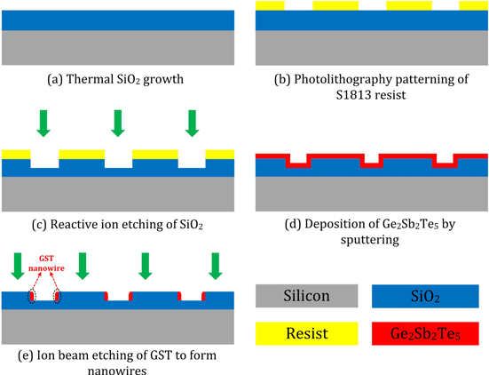
Figure 1. Fabrication process of spacer etch Ge2Sb2Te5 nanowires.
Download figure:
Standard image High-resolution image2.2. Fabrication and characterization of nanowire devices
The nanowire-to-TiN structure devices were fabricated by depositing and patterning TiN electrodes on two ends of the SiO2 trench by photolithography and lift-off processes. A negative nLOF AZ2070 resist was used in this photolithography process. This is followed by the deposition of the electrode film. Immediately before TiN film deposition, an Argon plasma treatment was given in the chamber to remove any native oxide and surface contamination on GST surface. Subsequently, 125 nm TiN film electrodes were deposited using medium frequency plasma assisted magnetron sputtering (Leybold Optics HELIOS Pro XL) at room temperature. This process combines reactive middle frequency sputtering with an additional RF plasma source. During each rotation of the plate holding the substrate, a thin layer of Ti was deposited from dual magnetron metal targets (99.99% purity) using a power of 3000 W in an Ar atmosphere. The thin film was then transformed into a nitride layer by passing the substrate underneath the N2 plasma of the RF source. The N2 and Ar flow rates were maintained at 30 and 35 sccm, respectively, and a high drive speed of 180 rpm was applied to enhance the film uniformity. The TiN electrodes were then fabricated using an acetone lift-off process.
3. Results and discussions
3.1. Spacer etch nanowire
Figure 2(a) shows a cross-section scanning electron microscope (SEM) image of a sample after GST film deposition over the SiO2 step. The GST layer can be identified on top of the thermal oxide layer and is about 110 nm in thickness. The GST film thickness on the sidewall was measured to be 50 nm and is reduced due to the non-conformity of the sputtering process. This region of the GST will eventually form the spacer nanowire after etching.
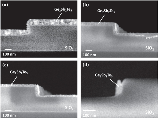
Figure 2. Cross-section SEM images of samples (a) before GST spacer etch, (b) after a 30 s etch, (c) after a 50 s etch and (d) after a 80 s etch. The nanowire is obtained after 80 s etch and the cross-sectional dimension of the nanowire is measured to be 50 nm × 100 nm (width × height).
Download figure:
Standard image High-resolution imageFigure 2(b) shows a cross-section SEM image of the sample after a 30 s etch. A clear decrease of the GST layer thickness from 100 nm to 55 nm can be observed. Additional etching of 20 s further decreased the film thickness while the GST along the sidewall remained untouched as shown in figure 2(c). After another 30 s etch, the GST on the planar surface has been completely removed (figure 2(d)), leaving a GST nanowire along the SiO2 step. The dimensions of the nanowire was measured to be 50 nm × 100 nm (width × height) which match the GST film thickness on the sidewall and the SiO2 trench depth, respectively, indicating that the nanowire dimensions can be precisely controlled by the fabrication process. The nanowire height is determined by the height of SiO2 step and can be controlled during the RIE process. The nanowire width is tuneable through the thickness of the deposited GST layer. The nanowire length is determined by the length of SiO2 trench.
The continuity of the nanowires was investigated by observation under optical microscope using differential interference contrast mode. Figure 3(a) shows a Nomarski micrograph of spacer etched GST nanowires. A clear contrast can be observed between the SiO2 trenches and the GST nanowires adjacent to their boundaries. All nanowires appear to be continuous with no evidence of discontinuities. A high magnification SEM image of a single GST nanowire is shown figure 3(b). The width of the nanowire is measured to be 48 nm which matches the data obtained from the cross-section SEM. It is worth mentioning that the nanowire shows some roughness which is attributed to the sidewall line edge roughness of the SiO2 trench. This could be further improved through a higher resolution photolithography process.

Figure 3. (a) Nomarski micrograph of spacer etch GST nanowire, nanowires can be observed at the edge of SiO2 trenchs; (b) SEM image of one spacer etch GST nanowire with line edge roughness.
Download figure:
Standard image High-resolution image3.2. Contact resistance
3.2.1. Phase change property
Two-terminal devices were fabricated in order to study the electrical properties of the nanowires and contact resistances. Figure 4 shows a fabricated nanowire device with several parallel nanowires obtained from SiO2 trenches. It is obvious that two identical nanowires are formed within each SiO2 trench. Two ends of the nanowires were covered by TiN electrodes, leaving an active nanowire length of 20 μm. Different contact areas can be obtained by incorporating several SiO2 trenches into one device. It is worth mentioning that the contact area of this device cannot be calculated directly from the total surface area of all nanowires covered underneath the TiN electrodes as the distribution of current density is not uniform within this area and additional care has to be taken in calculating the actual contact area for this device. Here we used COMSOL to simulate the current distribution between the TiN electrodes and the GST nanowires. A single GST nanowire device structure was first built in COMSOL based on the actual dimensions of the device. A DC bias of 10 V was then simulated on two TiN electrodes while the resultant current density distribution between the TiN electrodes and GST nanowires was used to determine the effective contact area. The results revealed that for each single nanowire, current flow from TiN electrodes to the nanowires were within an area of 75 nm × 150 nm away from the edge of the TiN electrodes. The actual contact area for one device can then be calculated from this effective contact area of each nanowire and the number of nanowires.
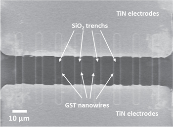
Figure 4. A fabricated nanowire device with several parallel nanowires. The effective length of the nanowire is 20 μm and is determined by the distance between two TiN electrodes.
Download figure:
Standard image High-resolution imageThe current-voltage (I–V) characteristics of the devices were measured using a DC sweep on the two TiN electrodes by an Agilent B1500A semiconductor device analyzer attached to a Cascade probe station. The phase change property of the nanowires was characterized first to evaluate the potential degradation of the GST material during the ion beam etching process. A DC sweep from 0 to 10 V was carried out on amorphous (as-deposited) devices with a length of 20 μm. It is worth mentioning that this voltage is much lower than the threshold voltage and will not induce any switching behavior [12]. The same devices were then annealed in N2 ambient at 200 °C (above the crystalline temperature of GST) for 5 min to crystallize the GST nanowire. The annealed devices were subsequently characterized under the same DC sweep condition.
Figure 5 shows current/voltage measurement of devices with nanowires in parallel of 20, 50 and 100 before and after annealing, all with an effective length of 20 μm. Devices before the annealing (figure 5, solid lines) give low currents and the resistance are extracted to be about 200 MΩ for device with 20 NWs. Devices after the annealing (figure 5, dashed lines) give significantly high current and the extracted resistances was found to be about 130 MΩ for the same device, significantly lower than results before annealing. This gives a resistance ratio of around 103 between the as-deposited and annealed devices which is similar to that for other memory cells with similar architectures fabricated from these PCM [13]. This suggests that the phase change property was well retained during the etching process.
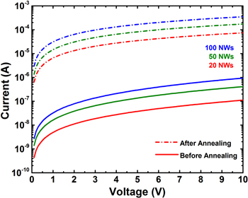
Figure 5. I–V characteristic of GST nanowires devices with 20 (red), 50 (green) and 100 (blue) nanowires in parallel in both amorphous state (before annealing, solid lines) and crystalline state (after annealing, dotted lines). The effective length is 20 μm for all devices.
Download figure:
Standard image High-resolution image3.2.2. Contact resistance for crystalline GST
In order to study the GST-TiN interface property, the I–V characteristics are re-plotted on a linear scale. I–V curves of crystalline GST nanowires are shown in figure 6(a) and display a linear relation for all three different contact areas. This linear I–V curve indicates an Ohmic contact between crystalline GST nanowire and the TiN electrodes and hence can be analyzed using a modified transmission line model (TLM) method [14]. The TLM method is a well-known simple and reliable technique for measuring both the contact resistance at a metal/semiconductor Ohmic interface and the resistivity of the semiconductor. The traditional TLM measures the resistance of a thin film semiconductor, while in this work we modified this model to adapt to our nanowire devices. We assume that the other parasitic resistances such as the TiN layer to be negligible as the used TiN is much more conductive (ρTiN = 85 μΩ cm in this work) than both crystalline and amorphous GST. The total resistance ( ) then only consists of the resistance of nanowire (
 ) and the two GST-TiN electrode contacts (
 ) and can be written as:

where  is the resistivity of GST in crystalline state;
  is the cross-section area of the nanowire devices which can be calculated from the cross-section of each nanowire and the number of nanowires,
  is the length of nanowires which is determined by the distance between two TiN contacts as discussed above,
  accounts for the specific contact resistance between GST nanowire and TiN electrode and
  is the contact area.
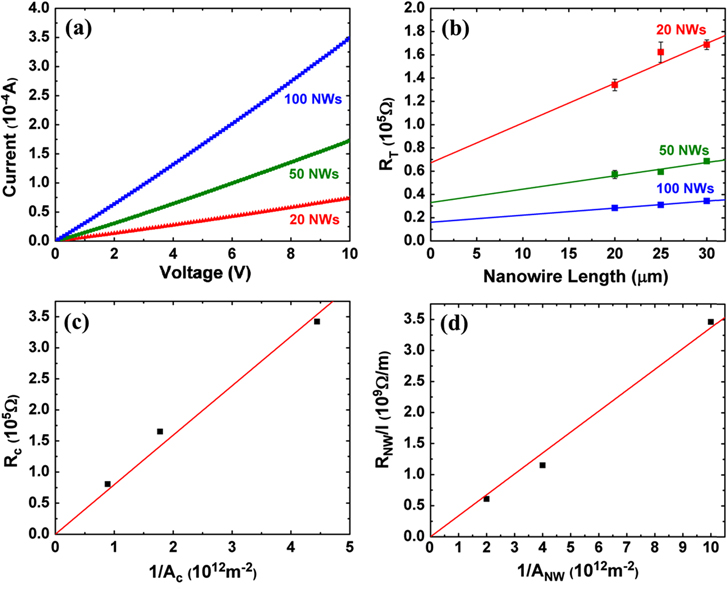
Figure 6. (a) I–V curves of crystalline GST nanowire devices with 20, 50 and 100 nanowires; (b) total resistance  as a function of nanowire length; the gradient and intercept of each linear fit represent nanowire resistance per length and contact resistance
  , respectively; (c) contact resistance
  versus contact area; the gradient is the specific contact resistance between TiN and crystalline GST; (d) nanowire resistance per length versus nanowire cross-section; the gradient is the resistivity of crystalline GST.
Download figure:
Standard image High-resolution imageTLM analyses were carried out using nine different combinations of the devices geometries with three different nanowire lengths (20 μm, 25 μm and 30 μm) and three different contact areas (20 NWs, 50 NWs and 100 NWs). For each combination, DC sweep measurements were made on several copies of identical devices. The total resistances were calculated from the linear fit of the I–V curve of each device. The average result for each combination is plotted in figure 6(b) with resistance against nanowire length. For three sets of devices with different contact areas, resistances obtained from three different nanowire lengths all display linear  relations with pronouncedly positive slopes which further prove the validation of the TLM for this work. The interception of each linear trend line corresponds to the contact resistance for each contact area. It is evident that the contact resistance plays an important part in the total resistance and its contribution to
  increases with an increasing nanowire numbers. The resulting relation of contact resistance and contact area is shown in figure 6(c). A linear relation between
  and
and  is observed which matches the relations indicated in equation (1). The specific contact resistance is 7.96 × 10⁻⁵ Ω cm2 from the linear fit. The resistances originating from the nanowires are extracted from the gradients of the linear fitted lines in figure 6(b) where each gradient accounts for the nanowire resistance per length. By plotting
  against
  as shown in figure 6(d), another linear fit was observed and the GST resistivity was found to be 3.37 × 10⁻² Ω cm.
3.2.3. Contact resistance for amorphous GST
Unlike in the crystalline state, the I–V characteristics of the GST nanowire device in amorphous indicate nonlinear conductive behavior of amorphous GST with TiN electrode as shown in figure 7(a). Good linear fits are obtained for all devices with different contact areas in a  plot (not shown), which is explained well with the following equation of Schottky emission conduction mechanism [15]:

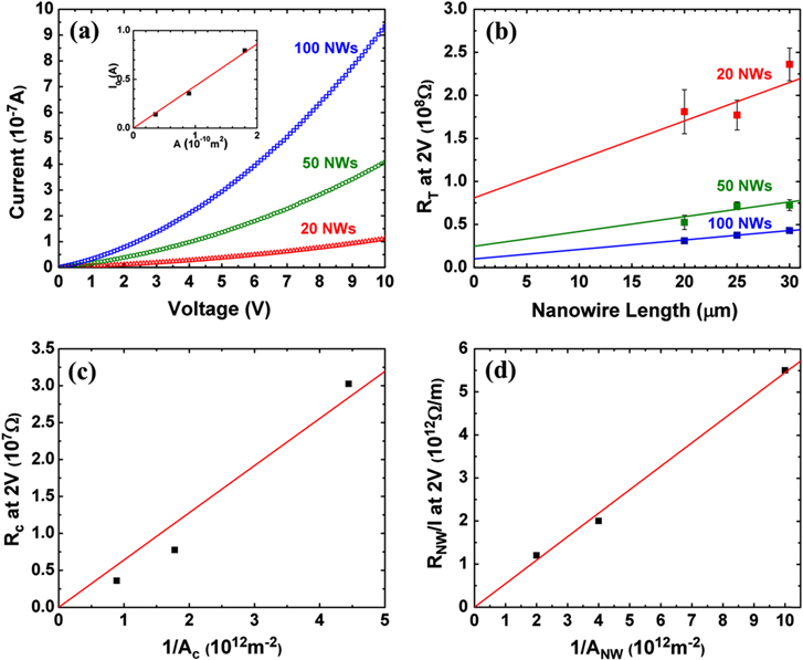
Figure 7. (a) I–V curves of amorphous GST nanowire devices with 20, 50 and 100 nanowires; the inset is a linear fit of the thermal stimulated current as a function of contact area A; (b) total resistance  as a function of nanowire length under a 2 V applied voltage; the gradient and intercept of each linear fit represent nanowire resistance per length and contact resistance
  , respectively; (c) contact resistance
  versus contact area; the gradient is the specific contact resistance between TiN and amorphous GST; (d) nanowire resistance per length versus nanowire cross-section; the gradient is the resistivity of amorphous GST.
Download figure:
Standard image High-resolution imagewhere E is electrical field, q is the electronic charge,  is dielectric constant of the material, k is the Boltzmann's constant, and T is absolute temperature.
  is known as the thermal stimulated current when no voltage is applied. The value of
  can be calculated from the intercept of each fitted line and has an expression of

in which A is the contact area,  is Richardson's constant and
  is Schottky Barrier Height. Schottky barrier between crystalline and amorphous GeSb PCM has been suggested before [16]. Here this work proves the existence of Schottky barrier between the amorphous GST and TiN electrode. The value of
  can be derived by linear fitting
  as a function of contact area A as shown in the inset of figure 7(a). A good fit was observed and the Schottky Barrier Height
  was calculated to be ∼0.6 eV. This suggests a noticeable contribution of the Schottky barrier at the amorphous GST/TiN interfaces to the overall resistance. Similar behavior has also been observed in other metal/semiconductor memory device [17]. The disappearance of the Schottky barrier upon annealing could be due to the annealing process which is believed to improve the Schottky contacts between metal and semiconductor contacts [18], or due to the band gap reduction from amorphous state to crystalline state [19].
In order to calculate the specific contact resistance between amorphous GST and TiN, we measured the total resistance  under an applied voltage of 2 V. This voltage is small enough not to induce any switching or heating effect. The resultant
  of different devices are plotted in figure 7(b). Good linear fittings against the nanowire length are observed for all three sets of devices. This suggests that TLM method is still valid and could be used in calculating the specific contact resistance and resistivity for amorphous GST under a small applied voltage.
  between amorphous GST and TiN can be extracted from the intercept of each line. A specific contact resistance of 6.39 × 10⁻² Ω cm2 was obtained by linear fitting
  with a function of
  as shown in figure 7(c). The resistivity of amorphous GST was calculated by first extracting the value of nanowire resistance per length from the gradients of linear fitted lines in figure 7(b) and then plotting it against
  as shown in figure 7(d). A good linear fit is again observed and the resistivity of amorphous GST at 2 V applied voltage is 54.5 Ω cm.
All values obtained from this work are summarized and compared with reported values in table 1. It should be mentioned that the data from this works are from nanowire devices whilst those in literature are from thin film devices. For the resistivity of c-GST, this work gives a consistent result with that in [3] and [20] and much lower than [19]. The discrepancy could be due to growth of GST under different conditions. In addition, the electrical conductance of nanowires is expected to be different from those of thin films and this could also play a role in the discrepancy. The resistivity of amorphous GST has a wide range. Lower values of a-GST resistivity have also been reported ranging from ∼100 to 300 Ω cm [21–23].
Table 1. Resistivity ρ of GST and specific contact resistance ρC of GST-TiN in both crystalline and amorphous phases, compared with previous reports.
| Reference |
 (c-GST) (mΩ cm) (c-GST) (mΩ cm) |
 (a-GST) (Ω cm) (a-GST) (Ω cm) |
 (c-GST) (μΩ cm2) (c-GST) (μΩ cm2) |
 (a-GST) (mΩ cm2) (a-GST) (mΩ cm2) |
|---|---|---|---|---|
| This work (GST-TiN) | 34 | 54.5 (at 2 V) | 80 | 64 (at 2 V) |
| Roy et al (GST-TiW) [3] | 20 | 805 | 3.8 | 95 |
| Kato et al [19] | 500 | 3000 | N/A | N/A |
| Lee et al [20] | 20 | 2000 | N/A | N/A |
N/A: not available.
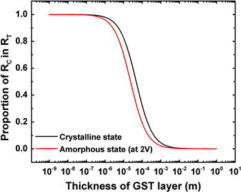
3.2.4. Proportion of  in
in


The proportion of contact resistance to the total resistance can then be calculated using the values obtained in this work. It is worth mentioning that in this work the contact area  is not as same as the cross-section area
  of nanowires allowing for an independent extraction of both values. For a conventional vertical phase change memory structure where the two areas are identical, proportion of
  to
to  can be calculated at different GST thicknesses using values obtained in our work. Note that here the GST thickness in vertical structure corresponds to the nanowire length in lateral structure. The proportion of contact resistance to the total resistance in such device is displayed in figure 8 as a function of different GST film thicknesses. It is evident that contact resistance dominates the total resistance for film thicknesses that are smaller than 1 μm in both crystalline and amorphous states. This indicates that in actual memory devices, the change in resistance between two phases is predominately an interfacial effect.
Figure 8. Calculated proportion of contact resistance ( ) in total resistance (RT
) for a conventional vertical GST device with different GST thicknesses.
) in total resistance (RT
) for a conventional vertical GST device with different GST thicknesses.
Download figure:
Standard image High-resolution image
4. Conclusions
A novel e-beam free, top-down fabrication process for a PCM nanowire is demonstrated using a spacer etch approach. According to the method, the dimensions and locations of the nanowires can be precisely controlled. It can be easily applied to other PCM and materials related to nanoelectronics. In addition, the contact resistance properties between nanowires and TiN metal contacts have been investigated. In amorphous state, a Schottky barrier of ∼0.6 eV between the interface of GST and TiN electrode is the main contributing factor to the total resistance of the devices. The specific contact resistance between GST and TiN electrode was found to be 7.96 × 10⁻⁵ Ω cm2 in the crystalline state and 6.39 × 10⁻² Ω cm2 in the amorphous state under an applied voltage of 2 V. These values are similar to those between GST and TiW electrodes. This work suggested that the contact resistance plays a dominant role in the total resistance of GST memory device in both crystalline and amorphous states.