Abstract
Photonic integrated circuits (PICs) are considered as the way to make photonic systems or subsystems cheap and ubiquitous. PICs still are several orders of magnitude more expensive than their microelectronic counterparts, which has restricted their application to a few niche markets. Recently, a novel approach in photonic integration is emerging which will reduce the R&D and prototyping costs and the throughput time of PICs by more than an order of magnitude. It will bring the application of PICs that integrate complex and advanced photonic functionality on a single chip within reach for a large number of small and larger companies and initiate a breakthrough in the application of Photonic ICs. The paper explains the concept of generic photonic integration technology using the technology developed by the COBRA research institute of TU Eindhoven as an example, and it describes the current status and prospects of generic InP-based integration technology.
Export citation and abstract BibTeX RIS

Content from this work may be used under the terms of the Creative Commons Attribution 3.0 licence. Any further distribution of this work must maintain attribution to the author(s) and the title of the work, journal citation and DOI.
Corrections were made to this article on 17 July 2014. Figures 27 and 28 were moved to their correct position in the article.
1. Background
1.1. History of photonic integration
After its first appearance in the published literature over forty years ago [1], it was believed that microphotonic integration would take a similar development path to that followed by microelectronic integration. In his review paper of 1977 Tien [2] mentioned as one of the major goals of microphotonic integration or 'Integrated Optics' as it was called at the time: 'the integration of a large number of optical devices on a small substrate, so forming an optical circuit reminiscent of the integrated circuit in microelectronics'. In the following years a number of chips of increasing complexity were reported. Figure 1 shows the complexity development measured as the number of components integrated on a single chip 17 . The underlying data is summarized in table 1 and briefly described below.
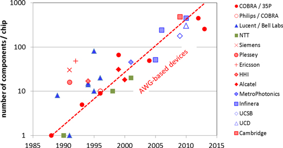
Figure 1. Development of chip complexity measured as the number of components per chip.
Download figure:
Standard image High-resolution imageTable 1. Development of chip complexity measured as the number of components (#Comp) per chip. The last column refers to the references listed at the end of this article.
| Year | #Comp | Short Title | 1st Author | Institute | References |
|---|---|---|---|---|---|
| 1988 | 1 | AWG | Smit | COBRA | [8] |
| 1989 | 8 | WDM source | Koren | Bell Labs | [3] |
| 1990 | 1 | AWG | Takahashi | NTT | [9] |
| 1991 | 30 | Grating Spectrograph | Cremer | Siemens | [4] |
| 1991 | 1 | AWG | Dragone | Bell Labs | [10] |
| 1991 | 16 | 4 × 4 Cross-bar switch | Duthie | Plessey | [5] |
| 1992 | 48 | Switch Array | Gustavsson | Ericsson | [6] |
| 1993 | 5 | WDM receiver | Amersfoort | COBRA | [11] |
| 1994 | 17 | Heterodyne receiver | Kaiser | HHI | [7] |
| 1994 | 14 | WDM laser | Zirngibl | Bell Labs | [14] |
| 1994 | 15 | WDM channel selector | Zirngibl | Bell Labs | [17] |
| 1995 | 10 | WDM receiver | Zirngibl | Bell Labs | [12] |
| 1995 | 81 | WDM receiver & preamp | Chandrasekhar | Bell Labs | [23] |
| 1996 | 9 | WDM receiver | Steenbergen | COBRA | [13] |
| 1996 | 20 | WDM laser | Zirngibl | Lucent | [15] |
| 1996 | 10 | WDM laser | Staring | Philips | [16] |
| 1998 | 10 | WDM channel selector | Ishii | NTT | [18] |
| 1999 | 66 | WDM cross-connect | Herben | COBRA | [22] |
| 1999 | 31 | WDM laser | Me´ne´zo | Alcatel | [19] |
| 2000 | 18 | WDM channel selector | Mestric | Alcatel | [20] |
| 2001 | 20 | WDM channel selector | Kikuchi | NTT | [21] |
| 2003 | 45 | WDM receiver | Tolstikhin | MetroPhotonics | [24] |
| 2004 | 49 | WDM receiver | 35 Photonics | 35Photonics | [25] |
| 2005 | 51 | WDM transmitter | Nagarajan | Infinera | [26] |
| 2006 | 240 | WDM transmitter | Nagarajan | Infinera | [27] |
| 2009 | 177 | Tunable WDM router | Nicholes | UCSB | [28] |
| 2009 | 480 | 16 × 16 SOA switch | Wang | UCAM | [29] |
| 2010 | 302 | Arb. Waveform Generator | Soares | UCD | [30] |
| 2010 | 450 | PM-DQPSK WDM transm | Corzine | Infinera | [31] |
| 2012 | 480 | 16 × 16 switch | Stabile | COBRA | [32] |
| 2013 | 256 | 8 × 8 wavelength switch | Stabile | COBRA | [33] |
Early examples of complex InP-based photonic integrated circuits (PICs) 18 are a WDM source by Koren [3], integrating three lasers consisting of a semiconductor optical amplifier (SOA) and a tunable Bragg Grating Reflector, with a power combiner and a booster SOA on a single chip; a grating-based receiver by Cremer [4], integrating an Echelle grating demultiplexer with more than 30 detectors; a 4 × 4 cross-bar switch by Duthie [5], integrating 16 reverse-Δβ switches; a switch array by Gustavsson [6], integrating 24 SOA gate switches with 24 1 × 2 couplers; and a polarization diversity heterodyne receiver by Kaiser [7], integrating a DBR-type local oscillator laser with polarization mode splitters, polarization mode filters, 3 dB combiners, detector diodes in balanced configuration, junction FETs and load resistors.
The highest complexities so far have been reported in AWG-based PICs. It started with the publication of the first AWG by Smit [8] in 1988, followed by Takahashi [9] and Dragone [10]. After the invention of the AWG a number of AWG-based devices with increasing circuit complexity were reported: WDM receivers with 5–10 components by Amersfoort [11], Zirngibl [12] and Steenbergen [13]; WDM lasers with 10–20 components by Zirngibl [14, 15] and Staring [16]; WDM channel selectors with 10–20 components by Zirngibl [17], Ishii [18], Ménézo [19], Mestric [20] and Kikuchi [21] and a cross-connect chip with 66 components by Herben [22]. A special device is the WDM-receiver with integrated pre-amplifiers by Chandrasekhar [23] which counts 81 components, most of them electronic (transistors and resistors).
Figure 2 illustrates two of these WDM devices: a WDM receiver with nine components (figure 2(a)) and a WDM cross-connect with 66 components (figure 2(b)).
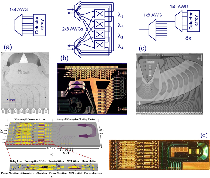
Figure 2. Examples of Photonic ICs: (a) a WDM receiver consisting of an AWG integrated with 8 detector diodes [13]; (b) a 4-channel 2 × 2 WDM cross-connect integrating 2 AWGs with 16 Mach–Zehnder interferometer switches in dilated configuration (66 components in total); (c) a 40-channel WDM monitor chip integrating 9 AWGs and 40 detector diodes [25]; (d) an 8 × 8 channel wavelength router, integrating 8 wavelength converter circuits with an 8 × 8 AWG, with over 175 components [28].
Download figure:
Standard image High-resolution imageThe new century brought a significant increase in complexity: WDM receiver and transmitter chips with 44–51 components by Tolstikhin [24], Three-FivePhotonics [25] and Infinera [26]. Shortly after, in 2006, Infinera published a 40-channel WDM transmitter with 241 components [27]. Figure 2(c) illustrates the 40-channel WDM monitor chip with 49 components [25] and figure 2(d) an 8 × 8 wavelength router chip with 175 components reported by Nicholes in 2009 [28]. In the same year Wang [29] reported a 16 × 16 SOA switch matrix with 480 components fabricated in an all-active wafer, and one year later Soares [30] a 100-channel Arbitrary Waveform Generator with more than 300 components. The latter device also contains 400 phase shifters for reducing the high cross-talk level in the very large AWG which is used to separate 100 wavelength channels. Two PICs with more than 450 components fabricated in an advanced active–passive integration technology have been reported by Corzine (Infinera) [31] and Stabile (COBRA) [32]. Stabile also reported an 8 × 8 wavelength switch with 256 components [33]. Table 1 gives an overview of the devices mentioned. An excellent overview of High Performance InP-Based Photonic ICs is given by Coldren [34].
In microelectronics there is a clear exponential development in the number of transistors per chip, which has been doubling every two years on average during the last four decades. This phenomenon is known as Moore's law [35, 36]. Figure 1 reveals a similar development in microphotonics, albeit in an early stage and with a much larger scatter than its microelectronic counterpart. If we restrict ourselves to devices based on AWGs, with a more or less comparable technology (AWGs with integrated amplifiers and/or detectors) most of the outliers disappear, however, which suggests that photonic integration is taking a similar development path to microelectronics, probably driven by the same improvements in process equipment.
1.2. Generic photonic integration technology
Despite similarities in the development of chip complexity there is, however, a marked difference between today's microphotonics and microelectronics, and that is in the R&D methodology followed. In microphotonics most integration technologies are developed and optimized for a specific application. As a result we have almost as many technologies as applications, most of them very similar, but sufficiently different to prevent easy transfer of a design from one fab to another. Owing to this huge fragmentation, the market for many of these application-specific technologies is too small to justify their further development into a low-cost industrial volume manufacturing process. And as a result the chip costs remain too high to find wide application.
This is quite different from microelectronics where a huge market is served by a small set of integration processes (most of them CMOS processes). In these processes a broad range of functionalities can be realized from a small set of basic building blocks (BBBs), like transistors, resistors, capacitors and interconnection tracks. By connecting these building blocks in different numbers and topologies we can realize a huge variety of circuits and systems, with complexities ranging from a few hundred up to over a billion transistors. We call such a process, in which a broad range of functionalities can be synthesized from a small set of BBBs, a generic integration process.
In photonics we can do something similar, as illustrated in figure 3(a). An integration process with building blocks for controlling the basic properties of light: the amplitude, the phase and the polarization, can support a broad range of functionalities. Figure 3(b) shows a schematic picture of five different components integrated in a single generic integration process on an InP substrate. The example is taken from the process of the COBRA research institute of TU Eindhoven. The green layer is the waveguide layer that carries the optical waveguide modes (indicated by a white spot); the dark red layer in the centre of the waveguide layer is the optically active gain medium. With a good waveguide structure we can make interconnections, but also passive components like couplers, filters and demultiplexers. With optical amplifiers (SOA), phase modulators and polarization converters, for manipulating the amplitude, the phase and the polarization of the light, the technology can support a broad range of functionalities, as illustrated in figure 4.

Figure 3. (a) Basic building blocks in generic electronic and photonic integration processes. (b) Schematic cross-section of the basic building blocks in a generic photonic integration process.
Download figure:
Standard image High-resolution image
Figure 4. Examples of the functionalities that can be realized with (a) passive waveguides devices alone, or in combination with (b) optical amplifiers and (c) phase modulators.
Download figure:
Standard image High-resolution imageFigure 4(a) shows a few components that we can make with passive waveguides. The most important ones are MMI-couplers and AWG-demultiplexers. With deep-etched strong-confinement waveguides we can make MMI-reflectors and compact ring filters. Another important building block that we can make in a passive waveguide is a polarization converter. By placing it appropriately in a Mach–Zehnder interferometer (MZI) we can make polarization splitters and combiners, and by placing it halfway a polarization dependent component, the response of this component becomes polarization independent.
SOAs in combination with passive devices offer a broad range of functionalities, as illustrated in figure 4(b): Fabry–Perot (FP) lasers, multiwavelength lasers, ring lasers and, when used in combination with a wavelength tunable reflector, also tunable lasers. By using a short SOA section in reverse bias as a saturable absorber we can make picosecond pulse lasers. And a SOA in reverse bias can also be used as a detector.
Figure 4(c) illustrates some of the functionalities that we can make by combining phase modulators with passive devices: amplitude modulators, space switches, wavelength selective switches, such as WDM cross-connects and add-drop multiplexers. And by making use of the nonlinear properties of SOAs integrated in an MZI we can make ultrafast switches.
An advantage of generic integration technologies is that because they serve many different applications, they justify the investments in developing the technology for a very high performance and reliability at the level of the building blocks. This will make circuits realized in such a technology highly competitive. A single generic process will not be suited to all applications, of course. Just like in microelectronics we will need a few different generic technologies, optimized for different kinds of applications. But the number of generic technologies can be small, much smaller than the variety in today's technologies.
Further, in a standardized technology we can develop design libraries and a related software infrastructure for components or subcircuits that are used by many designers. This leads to a significant reduction of the design time and an increase in the design accuracy, so that fewer design cycles will be necessary to arrive at a required performance.
All this brings a fundamental change in the business model of photonics and allows commercial and academic groups to co-operate and move forward rather than forever reinventing the wheel.
1.3. Multi-project wafer runs
An important advantage of generic integration technology is that a number of different designs can be combined on the same wafer, because they all use the same fabrication process. Such a wafer is called a Multi-Project Wafer (MPW). And the Photonic ICs fabricated in such an MPW run are called ASPICs: Application Specific Photonic ICs, the photonic equivalent of an ASIC. ASPICs are application-specific PICs, realized in a standardized generic process. Figure 5 illustrates how a number of designs are combined on a single wafer. In this example there are 12 different designs; each design is repeated four times. So from each wafer in an MPW batch, the designer will receive four chips. This approach leads to a large reduction of the research and development costs. In the development stage often a few design and fabrication cycles are necessary to arrive at the required performance. Usually a few chips out of the wafer are sufficient for testing the design in this stage. By combining a number of designs on a single wafer every designer gets a few chips and the costs of the run can be shared by all participants in the MPW-run. This will lead to a more-than-ten-fold reduction of the costs of a design run.
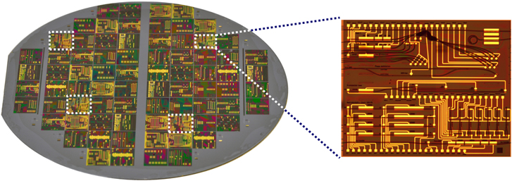
Figure 5. Example of a multi-project wafer (MPW) realised in the COBRA process. The wafer contains a large number of cells with different ASPICs. The wafer has 52 cells in the usable wafer area. Each ASPIC is copied at four different locations on the wafer, so that we have room for 12 users and one test cell, which is used for wafer validation. The figure shows one cell (a test cell) and its position on the wafer. In this way, each user will receive four copies of his chip per wafer in the MPW batch. COBRA usually runs two wafers in a batch.
Download figure:
Standard image High-resolution image1.4. Generic foundry model
The generic integration approach will lead to a large cost reduction by developing different products in a single or a few highly standardized processes. However, if the owner of the process does not provide access to external users the number of companies that can take advantage of this approach remains restricted. The corner stone of the generic foundry model is, therefore, the generic foundry: a chip manufacturer that provides open access to its generic integration process(es). In silicon microelectronics a number of chip manufacturers are providing such foundry access. In Photonics the generic foundry model is new.
The COBRA research institute of TU Eindhoven has been pioneering generic photonic integration technology since the beginning of the century [37]. The generic approach gained momentum in the European Network of Excellence ePIXnet [38], in which more than 63 research groups active in the field of photonic integration were cooperating in the period from 2004–2009 on a number of photonic integration technologies. InP-based generic photonic integration technology has been explored in a number of European and national projects 19 . Access to InP-based generic foundry processes is organized by the JePPIX platform [44], in which Europe's key players in the field of InP-based photonic integration technology are cooperating. A more detailed description of the InP-based generic foundry approach is given in Smit et al [45]. At present (semi-) commercial access to InP-based generic foundry processes is offered by three chip manufacturers: the UK-based company Oclaro, the Fraunhofer Heinrich Hertz Institut in Berlin and the COBRA spinoff company SMART Photonics, located in Eindhoven, the Netherlands, which is commercializing the COBRA process.
Figure 6 gives a (strongly simplified) explanation how the entry costs are reduced by the introduction of the generic foundry approach. In a vertical integrated fab model the component manufacturer owns the cleanroom facilities. The costs of a well-equipped cleanroom fab for fabrication of Photonic ICs are in the order of one or even a few hundred million Euros (or dollars) for advanced fabs. As shown in figure 6 chip volumes in excess of 10 million mm2 (2500 3'' wafers) are required to bring the investment cost per chip below 10 € / mm2. A chip with moderate complexity measures 10–30 mm2, so at this price level about one million chips are required for return of investment. Such investments are only affordable for market-dominant, top-tier technology companies.
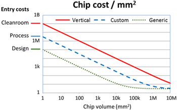
Figure 6. The dependence of chip costs on the production volume for three different manufacturing models: a vertical integrated fab model, a custom foundry model and a generic foundry model.
Download figure:
Standard image High-resolution imageA few cleanroom owners provide access to fabless customers in order to share the burden of the cleanroom operational expenditure. In this way a fabless customer can avoid the huge investment in a fab and restrict investment to just the development costs of a specific integration process for a specific PIC. We call this model the custom foundry model: the foundry develops application-specific processes for customized PICs. For PICs of moderate complexity the process development costs, including process qualification, are in the order of a million up to a few million Euros and the level of 10 € / mm2 is reached at volumes of a few times 10 000 chips (the second curve in figure 6 labelled custom). These are still significant volumes and the investment costs in combination with the risk are prohibitive for most small and medium enterprises (SMEs).
A dramatic further cost reduction can be achieved if the chip design is based on a generic (standardized) integration process, the development costs of which can be shared by many users. Then the entry costs are mainly restricted to design costs, which can be in the order of 100 k€. The design costs can be reduced even further by development of dedicated process design kits (PDKs) with component libraries that contain the mask layout and accurate models of the building blocks in the foundry platform. This will lead to both a reduction of the design time and the number of design cycles required to arrive at the required performance. In this approach, the cost level of 10 € / mm2 can already be reached at volumes of 1000 chips (the third curve in figure 6 labelled generic). It will make entry costs for development of Photonic ICs affordable for most SMEs. We expect, as a consequence, that the introduction of the generic model will lead to a rapid expansion in the application of Photonic ICs.
2. Generic integration process
There are many kinds of application-specific integration technologies, but also for the more generic technologies there is a large freedom in integration concepts, and different foundries will have different integration technologies, even if they are functionally equivalent. In this section we will explain the basics of a generic photonic integration process using the COBRA process as a representative example; it was the first generic process that offered an MPW service and most of the process and building block information is already in the public domain.
The integration process can roughly be subdivided into four process modules, which are illustrated in figure 8 and will be described below in broad outline. We will also indicate some new developments that are presently underway or planned for the continued evolution in generic processes at the JePPIX foundries Oclaro, Fraunhofer HHI and SMART Photonics.
2.1. Epitaxial growth
For the integration of active (amplifier) and passive (transparent waveguide) materials a number of integration schemes have been reported, which can be divided into single and multistep epitaxial growth processes.
Single step epitaxial processes. In single-step processes the full layer stack, including active and passive layers is grown in one single epitaxial step and the transparent waveguide sections are created afterwards by locally removing the active layers, as shown in figures 7(a) and (b). Figure 7(a) shows an active waveguide on top of a passive waveguide. In this approach special structures, e.g. vertical tapers, are required for coupling the light smoothly from the active to the passive waveguide and vice versa. A detailed description of a vertical integration approach is given in Menon [46] and Tolstikhin [47]. In figure 7(b) there is only one (composite) waveguide, which includes the active layer. So no vertical coupling is needed, but at the expense of a discontinuity between the active and the passive waveguide section which causes coupling loss and reflection. The discontinuity can be reduced by covering the structure with an InP cladding layer, but this requires an additional growth step.

Figure 7. Four active-passive integration schemes: (a) vertical twin-guide integration, (b) vertical single guide integration, (c) quantum well intermixing (and selective area growth), (d) butt-joint integration.
Download figure:
Standard image High-resolution imageFigure 7(c) illustrates another single-step integration method: quantum well intermixing. Here the active layer consists of a number of quantum wells. The active layer can be made passive by capping it with a material which generates vacancies in the semiconductor crystal that diffuse to the active layer when the wafer is heated. These vacancies cause the quantum well atomic species to intermix with those of the barrier layers between them which leads to an increase of the effective bandgap. Intermixing can increase the band gap wavelength of the active material by more than 100 nm, so that it becomes fully transparent. But also intermediate values are possible, e.g. for use in electro-absorption modulators. A detailed description is given by Skogen [48]. One of the disadvantages of this method is that the dopant concentrations in the active and the passive regions are the same, which causes high losses in the transparent regions. This problem can be solved by introducing an additional epitaxial step for growing an undoped cladding layer on the transparent waveguide section (blanket growth).
Multistep epitaxial growth processes. Single step processes are simple from an epitaxial point of view, but efficient and well controlled coupling between the active and the passive parts introduces additional complexity in the form of taper structures and/or additional growth steps. Figure 7(d) illustrates the most frequently applied approach: butt-joint integration. Here the active and passive waveguide structures are created in different growth steps, thus providing a large flexibility in the epitaxial layer structure and in the doping levels. In the past the additional growth stages could cause serious yield problems, however, with modern epitaxial technology this is no longer an issue.
In the COBRA generic process a three step epitaxial process is used to obtain the structure depicted schematically in figure 7(d), and in more detail in figure 8(a).
Figure 8. Cross-section of the wafer structure after the four process modules: (a) epitaxial growth, (b) waveguide etching, (c) passivation and planarization, (d) contacting and interconnect metallization.
Download figure:
Standard image High-resolution imageIn a first growth step the active layer stack is grown including the lower part of the p-doped cladding. Next the active regions are masked and the exposed area is etched away. In a second selective area regrowth step the etched-away part is replaced with a transparent waveguide stack, up to the same level as the first growth. In the transparent part the cladding layer is not doped in order to avoid absorption loss incurred by the p-dopant. In a third growth step the whole structure is covered with a p-doped cladding layer. If the regrowth process conditions are properly tuned the regrown wafer has a smooth surface and a smooth connection with low reflectivity between the active and the passive waveguide. Tapered and tilted interfaces are beneficial for further reduction of optical losses and reflections.
The processes at COBRA and Oclaro are very similar in outline, although different in detail. The process of Fraunhofer HHI differs more: it uses a semi-insulating (Fe-doped) substrate which leads to better rf-capabilities and enables electrical isolation of individual devices as required for example in balanced detectors. As yet it does not support the integration of optical amplifiers, but future releases of the platforms will offer a similar functionality, with differences in the technological details. In the following paragraphs we discuss a number of process enhancements that are presently being investigated.
Reduction of waveguide loss. In the present integration scheme, the p-doped top cladding, which is required for electrical connection to the active components, introduces an additional waveguide propagation loss of the order of 2 dB cm−1 for an optimized layer stack design. In larger PICs, which may have several centimetres of waveguide length, this introduces high losses. This loss contribution can be removed by restricting the p-doped cladding layer to the active regions, thus having no p-dopant in the transparent waveguide sections. Losses in the undoped regions are below 1 dB / cm, and the active regions are usually so short that the additional loss contribution due to the p-dopant is a few tenths of a dB at most. A locally undoped cladding layer can be realized by an additional growth step for the transparent waveguide sections or by incorporating the dopant only at the active regions by diffusion through a mask. COBRA is working on development of a low-loss generic process based on the latter approach.
Improving rf-performance. An important improvement of the performance can be obtained by fabricating the whole circuit on a semi-insulating (SI) substrate instead of an n-type substrate, as is presently already done by HHI for its high-speed receiver process. Moving from n-type to SI-substrate requires a redesign of the process, in order to replace the common n-contact at the backside of the wafer by lateral n-contacts which can be accessed from the top of the wafer. An SI-based process brings two advantages. The removal of the conductive n-type ground plane allows for higher speed operation. Both detectors and modulators on SI substrates can operate at frequencies beyond 40 GHz. Further, the n-contact layers of different components can be separated, which allows for integration of balanced photodetectors, where the p-contact from one diode is connected to the n-contact of the other. Oclaro and COBRA are both working on introduction of generic processes on SI substrates.
Free choice of bandgap. Another important extension of the platform capability is to allow a free choice of the bandgap of the active material. At present the same platform process can be applied to source wafers with gain sections containing different gain materials, e.g. bulk, Quantum Well or Quantum Dot layers, but only a limited number of vertical structures can be realized on the same wafer (typically 2 or 3). Hence, in MPW runs a choice has to be made which applies to all participants in that run, there is no flexibility within one chip or wafer.
A process offering more flexibility in bandgap properties is selective area growth (SAG). Here the growth rate in the active regions is enhanced by masking the area besides the active region. During MOVPE growth, species migrate from the masked areas to the unmasked areas where the growth rate becomes higher. If the waveguide consists of an MQW stack the wells in the active region will become thicker and this will lead to a reduction in the bandgap. The reduction can be controlled by controlling the growth enhancement via the width of the mask and the gap between the masked regions. In this way each active region can be controlled individually over a bandgap range as wide as 100 nm [49]. Because the bandgap changes are caused by a diffusion process the connection between regions with different bandgap will be smooth. In order to prevent the variations in layer thickness getting too large the SAG step is usually restricted to the active layer and the cladding layer is grown in an unmasked step. SAG thus requires multiple growth steps.
In this way a whole range of vertical structures can be designed on the same MPW which gives the designer a large degree of freedom in design of active layer properties. Firstly, the vertical structures can be optimized for multiple functionalities on the same wafer: lasers, semiconductor amplifiers, electro-absorption modulators, phase modulators, passive waveguides, etc. Secondly, the layer stacks can be optimized for each operating wavelength. For example in a WDM transmitter PIC, each laser and each electro-absorption modulator can be optimized individually for each wavelength channel. In the PARADIGM project, III–V Lab is cooperating with Fraunhofer HHI to implement this technology in a future release of their generic platform technology. In this release active MQW structures made of InGaAlAs rather than InGaAsP will be used for improved high-temperature operation.
2.2. Waveguide etching
The second process module is the waveguide etching. In the COBRA process four etch steps are used for creating four different etch levels, as shown in figure 8(b). The deepest level stretches into the substrate and is used in the deep etched waveguides, in deep-etched phase modulators and detector sections (reverse biased SOA sections), and for providing high index contrast. The deep etched waveguides are used where high contrast is essential, e.g. in small-radius bends and in compact MMI-couplers, MMI-reflectors and AWG-(de)multiplexers.
The shallow etch level is used for defining shallow etched waveguides and amplifier sections, where etching through the active regions would cause increased surface recombination. Shallow waveguides show lower propagation losses due to reduced sidewall scattering; they are used for low loss interconnections.
A third etch level is applied for providing electrical isolation between different active components. The isolation is achieved by removing the highly conductive p-doped top cladding layer, down to the low-doped cladding layer just above the waveguide layer. Further, as shown in figure 3(b), this level is used in the polarization rotation sections.
The fourth and shallowest etch step is used for removing the heavily p-doped ternary (InGaAs) contact layer from the passive waveguides, where it contributes to the waveguide losses. Further, after planarization, it allows for routing electrical interconnections across the waveguides, as shown in figure 8(d). This is important because it allows routing of the electrical connections to the edge of the chip.
DUV lithography. The quality of the waveguides and the components based on them, such as AWGs and MMI-couplers, is strongly dependent on the quality of the lithography and the etching process. COBRA has recently installed a 193 nm DUV scanner (ASML PAS 5550/1100) with a resolution down to 90 nm. The machine has been adapted by ASML for handling 3' and 4' InP-wafers, and so far it is the only machine with this resolution worldwide that can handle InP wafers. Resolution of this machine is three times better than today's best optical lithography tools for InP-wafers (I-line steppers), which have a resolution of 250 nm.
Such an increase in resolution leads to a large increase in process performance and platform capabilities. An important advantage is that DBR and DFB gratings can be printed with fast optical lithography instead of E-beam lithography or holography. But there are more advantages. The insertion losses of AWGs will reduce from a few dB to less than 1 dB by reducing the closure of the gaps between the array waveguides. With the improved resolution the control of critical dimensions in MMI couplers and polarization converters will become much better allowing more accurate specification of device performance and leading to higher yield. Also, it can be expected that the waveguide propagation losses will become lower due to smoother waveguide edges.
The very thin photoresists that are used for 193 nm DUV lithography are not suited as a mask for etching thick layers and do not tolerate height steps in excess of 100 nm. As can be seen in figure 8, after the first etch step the height difference will be many times larger. Planarization steps will, therefore, be required after each etch step, similar to what is done in CMOS processing. Also the requirements on wafer flatness are tighter than those that InP substrate manufacturers can provide today. Moving from I-line to 193 nm DUV lithography requires, therefore, major adaptions of the process technology. Such process adaptions are presently being investigated by COBRA, with support of ASML.
2.3. Planarization and passivation
After the etching process the sidewalls of deeply etched phase modulators and detectors have to be passivated and protected as shown in figure 8(c). In the COBRA process this is done by deposition of a polyimide layer which also reduces the height difference on the chip (planarization). The passivation layer is necessary for obtaining low dark currents in reverse biased phase modulator and detector sections. Planarization is necessary in order to facilitate subsequent lithography steps, where the large difference in height between the different mesas complicates process steps like opening of the contact regions and definition of metal contacts. The planarization layer is also used as a substrate layer for metal interconnect between electrodes and bond or probe pads. It has a well-defined height at all mesas where contacts openings have to be made and it covers the mesas where metal crossings are required for interconnect purposes.
As explained in the previous section introduction of DUV lithography imposes much more stringent requirements on the surface planarity. COBRA is working on development of chemical–mechanical polishing of a BCB planarization layer to meet those requirements.
2.4. Metallization and interconnect
The last process module is for contacting and metallization as shown in figure 8(d). First the polyimide planarization layer is patterned lithographically and the remainder is etched back until the active mesas are opened. Next a thin Ti-Pt-Au contact layer is deposited with lift-off lithography for getting contacts with low series resistance. The alignment is not critical because the contacts are chosen wider than the mesa. After lift-off of the front contact the backside contact is deposited. Both contacts are annealed at the same time. For definition of bond pads and metal interconnect patterns the upper side of the wafer is covered with a thin gold seed layer, followed by a thick resist layer, which is opened where we need the metal paths. Next a thick gold pattern is electroplated through the openings in the resist mask and finally the whole gold pattern is etched back a little bit in order to remove the seed layer.
3. Building blocks
3.1. Introduction
The basic idea behind a generic integration technology is to support the monolithic integration of a small set of accurately characterized building blocks that offer the basic functionality which is required to realize PICs for a broad range of different applications. Although the basic idea looks simple, its practical elaboration is not so straightforward, because the number of building blocks tends to become large: different types of lasers (FP, DFB, DBR, CW, pulse, tunable etc), modulators, detectors, MMI-couplers (1 × 2, 2 × 2, 1 × 4, 2 × 4, 4 × 4 etc) and AWGs with varying numbers of channels and channel spacings, to mention just a few. To utilize the full potential of the generic integration technology these building blocks have to be accurately characterized so that users can accurately design complex circuits based on them. A user designing a circuit based on these standard components will quite rightly ask for a guarantee from the foundry that the building blocks perform according to an agreed specification. Validating the proper performance of fabricated wafers will place a huge burden on the fab if approached in the wrong way, because the whole set of building blocks should be guaranteed for each MPW. Further, with so many different building blocks it will become a complex task to optimize the integration process: which building blocks should get priority in the process development?
In order to make the generic process development and validation manageable we distinguish between basic building blocks (BBBs) and composite building blocks (CBBs). The idea is to identify a small number of BBBs, which can be used to construct a much larger variety of building blocks which are composed of BBBs: CBBs. In this way we create a hierarchy of building blocks in which the properties of the higher layers can be derived from the properties of the lowest layer, the BBBs. The scheme is depicted in figure 9; it will be explained in some detail in the following sections.

Figure 9. Schematic diagram of the hierarchical structure for the different building blocks. (a) The basic building blocks offer the basic functions available on the platform. A number of BBBs can be combined in composite building blocks that perform more complex functions. They may also contain other CBBs. CBBs can have different levels of complexity, varying from a few up to a few hundred BBBs. (b) The Basic Building Blocks form the lowest functional level of the platform. At a process technology level a number of BBBs with different functions may be realized from a single structure, which we call a basic technology block.
Download figure:
Standard image High-resolution imageWith this subdivision the optimization and the validation of the generic process can now be focused on a small set of building blocks: the BBBs. If their performance is optimized and validated, the performance of all PICs that are built from them according to the design rules should also meet the expectations. So instead of optimizing and validating a process for a huge number of different components, the foundry can focus all its efforts on optimizing and validating a small set of BBBs, which significantly reduces the technology development and validation burden.
3.2. BBBs
BBBs are the smallest (irreducible) set of functional building blocks that are required to realize the full functionality provided by the generic technology. If a building block can be decomposed in more elementary building blocks then it is not a BBB but a CBB. A laser, for example, is composed of a gain section and a resonator, so it is a CBB. The resonator itself can be formed by a ring cavity, a FP cavity (two mirrors) or a Bragg grating. For an FP-laser, for example, the BBBs are a SOA section to provide the gain, and cleaved facets to form the cavity. The SOA and the cleaved facets are BBBs since they cannot be decomposed into more elementary building blocks. A ring resonator is composed of curved and/or straight waveguide sections, so it is a CBB. The straight and curved waveguide sections themselves are BBBs. The arrows in figure 9(a) illustrate how a CBB can be composed of a number of BBBs and/or CBBs.
Below a short description is given of the most important BBBs available in the present generic integration processes at Oclaro, Fraunhofer HHI and COBRA/SMART. Although the different processes have a lot of BBBs in common, their performance may differ, and they can also offer some building blocks that are not offered by the other platforms. Further, some building block epi-structures can be exploited to provide several different functions, a point which is expanded upon in section 3.4 below. Table 2 gives an overview of the different BBBs.
- (1)Passive waveguide section (WG). Transparent waveguide sections are the most elementary building block in any generic process. They are used for interconnects and in CBBs such as MMI-couplers and AWGs. They can be provided with different optical confinements, e.g. deep or shallow etched for strong or weak confinement. Their most important property is the propagation loss, which should be as low as possible.
- (2)SOA. An SOA is an active waveguide section which provides gain to the guided signal when an injection current is applied. Furthermore the nonlinear operation of this BBB is interesting for many applications, e.g. in all-optical switching.
- (3)Saturable absorber (SA). This is a reverse biased pin-doped absorbing waveguide section, which becomes transparent if sufficient e–h pairs are generated by the absorbed light to get population inversion (bleaching). A short reverse biased SOA-section can be used as an SA.
- (4)Waveguide photo detector (PD). A waveguide PD is an absorbing waveguide section provided with electrodes to carry the photocurrent. Its structure closely resembles that of an SOA and a short reverse biased SOA section can be used as a detector.
- (5)Electro-refractive modulator (ERM, ERMI). This is a pin-doped waveguide section in which a reverse (ERM) or a forward bias voltage (ERMI, current injection) induces a phase shift. The physical effects under reverse biased operation are very fast. With proper electrode design modulation as fast as 40 Gb s−1 is possible. With current injection the speed is restricted to a few Gb s−1 by the carrier recombination time.
- (6)Electro-absorption modulator (EAM). Electro-absorption modulators are amplitude modulators. They operate at the band edge and use its bias-voltage dependence to modulate the absorption. They require a special pin-doped waveguide stack with a different epitaxial structure, which is not available in the present foundry platforms. HHI has planned it for a future platform release. Modulation speed in excess of 40 Gb s−1 has been reported.
- (7)Thermo-optic modulator (TOM). A thermo-optic modulator is a passive transparent waveguide section for which the phase transfer can be changed by heating it with a heater electrode on top of the waveguide. Modulation speeds are in the millisecond range.
- (8)Tunable Bragg reflector (TBR). This is a pin-doped waveguide section with a periodic corrugation for which the peak reflection wavelength can be tuned by changing the bias current. It is a key device in tunable DBR or DFB lasers.
- (9)Electrical isolation section (EI). This is a waveguide section in which the highly p-doped top cladding has been removed or made highly resistive by proton implantation. It is used, for example, for isolating a forward biased SOA section followed by a reverse biased phase modulator from each other. Without such a section electrical cross-talk will reduce circuit performance.
- (10)Polarization rotation section (PR). This is an asymmetric waveguide section (e.g. with an angled waveguide side wall) that has rotated modes and a strong birefringence. It can provide polarization rotation when properly connected to normal waveguides.
- (11)Spot-size converter (SSC). This is a BBB that adapts the size of the mode in the output waveguides of the PIC to better match the mode of a cleaved or lensed optical fibre or a dielectric interposer chip. In the current platforms these BBBs all use smoothly varying tapered waveguide cross-sections to achieve this function.
- (12)Waveguide termination (WGT). This is a device which is used for coupling light out of the PIC or for providing a low or high-reflection termination. It can be a simple cleaved facet or an etched facet, straight or angled (the latter for reducing reflection), and it may contain a high-reflection or anti-reflection coating.
Table 2. Overview of the basic building blocks available in the three foundry platforms, at present and planned for 2015.
| 2012 | 2015 | |||||||
|---|---|---|---|---|---|---|---|---|
| Basic building blocks | Abbr | Oclaro | HHI | COBRA | Oclaro | HHI | COBRA | |
| 1 | Passive waveguide | WG | • | • | • | • | • | • |
| 2 | Semiconductor optical amplifier | SOA | • | • | • | • | • | • |
| 3 | Photo detector | PD | 10 GHz | 40 GHz | 10 GHz | 40 GHz | 40 GHz | 40 GHz |
| 4 | Saturable absorber | SA | • | • | • | • | • | |
| 5 | Electro-refractive phase modulator | ERM | 10 GHz | 10 GHz | 40 GHz | 40 GHz | ||
| 6 | Injection-type ERM | ERMI | 1 GHz | 1 GHz | 1 GHz | 1 GHz | ||
| 7 | Thermo optic phase modulator | TOM | • | • | • | • | • | • |
| 8 | Electro-absorption modulator | EAM | 25 GHz | |||||
| 9 | Tunable Bragg reflector | TBR | • | • | • | |||
| 10 | Electrical isolation section | EI | • | • | • | • | • | |
| 11 | Polarization Rotation section | PR | • | • | ||||
| 12 | Spot-size converter | SSC | • | • | • | • | • | |
| 13 | Waveguide termination | WGT | • | • | • | • | • | • |
3.3. CBBs
CBBs are building blocks that are composed by combining two or more BBBs and that do not require additional process steps for the combination. CBBs can be assembled by the designer using the design tools without reference to the process. For a number of them the name CBB is counterintuitive: most designers will consider a junction between two different waveguides, an MMI-coupler or a FP laser not as a CBB. As explained in the previous sections, in order to simplify the technology development and the process validation it is important to keep the number of BBBs as small as possible, and this can only be achieved if we label all components that can be formed from BBBs without further adaption of the technology as CBBs. So a laser and an MMI coupler are definitely CBBs. But also much more complex sub-circuits can serve as CBBs. Actually every sub-circuit that can be re-used as a building block in other ASPICS is a CBB. To enable its re-use it is important that it is made available to other users by including it in a component library that is provided to designers in the generic process: building an extensive CBB-library is an important target for generic platform technology development.
Where the distinction between BBBs and CBBs is not relevant we will call them just building blocks. Examples of CBBs are:
- (1)Junctions between a variety of waveguides:
- ▪Straight and curved waveguides
- ▪Waveguides with different (or opposite) curvature as used in S-bends
- ▪Waveguides with different widths (tapers)
- ▪Shallow and deep waveguides
- ▪Active and passive waveguides
- (2)MMI couplers, filters and reflectors:
- ▪Power splitters and combiners. Special case: 3-dB couplers.
- ▪MMI mode filters
- ▪TE–TM splitters and combiners
- ▪MMI-reflectors. These are MMI-couplers with a deep etched corner mirror at the end. They can be used as broadband on-chip reflectors.
- (3)AWG (de)multiplexers. Here a large variety in device specifications is possible: multiple input and output ports, different channel spacing, free spectral range (FSR), channel passband width and shape (parabolic or flattened).
- (4)Lasers, such as FP lasers, tunable DFB and DBR lasers and (Mode-Locked) pulse lasers.
- (5)Mach–Zehnder or Michelson interferometer (MI) modulators and switches
- (6)Switching matrices
- (7)WDM transmitters
- (8)Advanced receiver circuits, such as DQPSK or PM-DQPSK receivers
- (9)Actually any ASPIC can be used as a CBB in a more complex ASPIC.
BBBs and CBBs are made accessible for the designers by including them in a component library. The BBB library modules are provided by the foundries. The CBB library is expected to grow continuously, with a public and a designer-owned part. Designers can add their CBBs as modules to the component library and distribute them via the PDK on conditions that can be agreed between the owner of the module and the distributer of the Design Kit. In this way the library can be expanded with contributions from many designers. The potential of a generic integration technology is to a large extent dependent on the size and coverage of its CBB library.
3.4. Basic technology blocks (BTBs)
BTBs are physical structures that can have different functions and that, consequently, can be used in different BBBs. An example is a SOA: a short reverse biased SOA section can also be used as a detector. In table 2, the building block structures that can serve to create a number of different functions have been labelled in bold italics and the BBBs that can be derived from them in normal italics. It is seen that by realizing one or more BBBs from a single BTB the number of different technology blocks that the fabs have to integrate is reduced, which also reduces the complexity of the integration technology required. However, we will need to characterize their performance individually and provide different validation criteria. We will discuss two such BTBs below.
SOAs, if operated in reverse bias, can be used as detectors. If the active layer is bulk material, the detector performance can be quite good (bandwidth >25 GHz). If the active layer is based on QW or QD-material the optical confinement and hence the absorption is lower and the detector length needs to be longer, which reduces the bandwidth and increases the dark current. The same structure can also be used as a Saturable Absorber in a Mode-Locked Laser. By using advanced epitaxial technology that provides design freedom in the choice of the band gap of the active layer stack (SAG technology) the number of BBBs in a generic process can be even further reduced: Electro-Absorption Modulators and detectors can then also be realized in the same process as the SOAs.
Electro-refractive phase modulators can be used both with reverse bias (depletion mode) and forward bias (current injection mode). Properties (electro-optic efficiency and bandwidth) will be significantly different. Further, if the electrode design is sufficiently flexible for use as a heater, they can also be used as thermo-optic modulators.
If the lithography has sufficient resolution to support first order gratings (required resolution in the order of 100 nm) the phase modulators can also be used as tunable gratings, for example in DBR lasers. Usually these gratings are realized with E-beam or holographic lithography and epitaxial overgrowth techniques. If they can be realized with side-wall gratings in the same step as the waveguides, e.g. with DUV-lithography, we no longer need different technology steps for the phase modulators and the tunable gratings: they can be derived from the same modulator section used as BTB.
The BTBs lead to very useful simplification of the process technology by using a single structure for a number of different functions. Whether such combinations are possible or not depends on the specific platform technology. Because the BTBs support different functions and do not form a complete set, as illustrated in figure 9(b), the basic functionality cannot be formed by the BTBs but only at the level of the BBBs, as indicated in figure 9(b). For the designers, the functional BBB-level is the starting point for the design, and the way in which the BBBs are formed in the integration process is not relevant for them.
4. BBBs
In the following paragraphs we will discuss a number of BBBs in some detail. Examples are taken from the COBRA process, because this was the first generic process that offered MPW services and most of the process and building block information is already in the public domain. They are representative of the building blocks offered by the other generic foundry processes at Oclaro and Fraunhofer HHI. Access to the COBRA process is presently offered by SMART Photonics.
Under the header Other platforms we provide for each building block some information about the most important features of the Oclaro and the Fraunhofer HHI platforms, and we also discuss ongoing work on improvements which will become available in later releases of the three platform processes.
In 2014 the JePPIX platform has launched semi-commercial access to MPW-runs on platform processes of Oclaro, the Fraunhofer HHI and SMART Photonics. Semi-commercial means that the processes are not yet fully qualified (often referred to as 'beta release' for commercial devices). Numbers and features mentioned in the present text are, therefore, a snapshot, which will be subject to change. For more actual and extensive information about the process specifications the reader is referred to the Design Manuals and the process specifications, which are available via the JePPIX platform [44] under NDA.
4.1. Passive waveguide sections (WG)
Transparent waveguide sections (WG) are the most elementary building blocks in any generic process. They are used for interconnection purposes and in CBBs like MMI-couplers and AWGs. They can be available with different optical confinements (waveguiding strengths), e.g. deep etched strongly guided (WGS) or shallow etched weakly guided (WGW). Their most important characteristic is the propagation loss, which should be as low as possible. Weakly confined waveguides usually have the lowest propagation loss and are good for interconnecting, but they do not allow for small-radius waveguide bends. Strongly confined waveguides are preferred for compact components and small bending radii, but their propagation loss is usually higher.
Figure 10 (left, middle) shows the cross-sections of a deep (strongly confined) and a shallow etched (weakly confined) waveguide in the COBRA process. The waveguide layer is a 0.5 μm thick layer of Q1.25 bulk material. Q1.25 means lattice-matched quaternary material (InGaAsP) with a composition such that the band edge is at a wavelength of 1.25 μm. For shallow etched waveguides the ridge is etched 100 nm into the waveguide layer. Deep etched waveguides are etched down to >150 nm below the waveguide layer. Waveguide widths can be chosen by the designer, advised standard widths are 2 μm for shallow waveguides and 1.5 μm for deep etched waveguides.

Figure 10. Left: cross-section of three passive basic building blocks: a shallow etched waveguide (WGW), a deep etched waveguide (PWS) and an isolation waveguide section (EI). Right: SEM photographs of a deep and a shallow etched waveguide covered with polyimide (the apparent side wall angle is due to the perspective of the SEM photograph).
Download figure:
Standard image High-resolution imageThe propagation loss is caused by absorption losses due to free carrier absorption in the upper p-doped cladding layer and by scattering losses due to side-wall roughness of the waveguides. The cladding layers and the lower part of the waveguide layer are doped because the same waveguide structure is used in the phase modulators. The n-type dopant has no significant contribution to the losses, but the p-dopant has. The upper cladding has a stepwise graded doping profile; it is lowest close to the waveguide where it interacts most strongly with the guided mode. Its minimum level is determined by the electro-optic efficiency of the phase modulator, which requires the pn-junction to be close to the waveguide. Good e-o efficiency can be obtained with a doping level that brings a propagation loss about 2 dB cm−1. For shallow etched waveguides the scattering losses are low, total waveguide losses are about 3 dB cm−1. For deep etched waveguides with 1.5 μm width the total losses are about 4 dB cm−1. Lower losses (below 1 dB cm−1) are possible with a more advanced integration process, as explained in section 2.1.
The advised minimum bend radius of the shallow etched waveguides is 500 μm. Bend radii of deep etched waveguides can be as small as 10 μm. Below 50 μm, significant polarization conversion can occur at the junctions between straight and curved waveguide sections if the side walls are not perfectly vertical. In the COBRA process we saw no significant polarization conversion for radii down to 20 μm [50].
Effective refractive indices of the shallow waveguides are in the order of 3.25 at 1550 nm wavelength. The birefringence of the shallow waveguides (effective index difference between TE-and TM-polarized modes) is in the order of 6.10−3, which will cause a shift in the order of 3 nm (400 GHz) in wavelength sensitive devices like AWGs and DBR gratings. For deep etched waveguides it crosses zero at a waveguide width of 1.5 μm, but it is very sensitive to small width deviations. A width deviation of 50 nm already causes a (wavelength dependent) birefringence variation of a few times 10−4, corresponding to a TE-TM shift up to 100 GHz in an AWG.
Electrical isolation sections. The high dopant level of the upper cladding provides a resistive path between all active components connected by a waveguide, such as SOAs, detectors and modulators. If these components operate at different voltages (e.g. forward and reverse bias) large leakage currents can occur which may change the operating voltages over the components (cross-talk). To prevent such a leakage current an electrical isolation waveguide section (EI), as shown in figure 10, has to be inserted between the two components. The resistance of this section, which is strongly increased by removing the highly doped upper cladding, is in the order of 20 kΩ μm−1 section length. The isolation section has slightly increased propagation loss, so it should not be made longer than necessary. The transition between a waveguide and an isolation section also introduces small additional loss. Possible reflections at this interface are reduced using an angled isolation etch.
Other platforms. The Oclaro platform supports only deep etched waveguides, which are identical to the Phase Modulator sections. Waveguide losses are comparable to the COBRA platform: around 3 dB cm−1. The Fraunhofer HHI offers waveguides with three different etch depths (weak, medium and strong confinement). Propagation loss of the low confinement waveguides is between 0.5 and 1 dB cm−1, for the strongly confined waveguides it is in the order of 2 dB cm−1. COBRA is working on an improved platform with waveguide losses below 1 dB cm−1 achieved by restricting the p-doped material to the active components (SOAs and ERMs) and avoiding it in the passive waveguides, as described in section 2.1.
4.2. Optical amplifiers (SOA), photo detectors (PD) and saturable absorbers (SA)
An important feature of the butt-joint epitaxial regrowth process is the modular character of the gain block: the integration process is not sensitive to the composition of the gain blocks, as long as the total thickness of the active waveguide layer is not changed. The process can be used, therefore, for bulk active layers (120 nm Q1.25 material) as well as for Quantum Well (QW) or Quantum Dot (QD) active layers with different emission wavelengths. The active layers are embedded in a Q1.25 separate confinement layer, and the total thickness of the active waveguide stack is 500 nm. All layers have their gain maximum around 1550 nm at appropriate current injection levels.
For the MPWs the COBRA process uses an MQW layer with four QWs embedded in a 500 nm Q1.25 layer. The standard SOA ridge width is 2 μm. The SOA is shallow etched in the same etching step as the shallow waveguides. A shallow etch is applied in order to avoid the etch reaching into the active layer, which causes increased surface recombination. Figure 11 (left) shows the cross-section. An 800 μm long SOA section has a modal gain of 20 dB at an injection current of 120 mA.

Figure 11. Left: cross-section of a semiconductor optical amplifier (SOA), a waveguide photo detector (PD) and a phase modulator (ERM). Right: SEM photographs of a SOA, a phase modulator and a vertical side wall grating (the apparent side wall angle is due to the perspective of the SEM photograph).
Download figure:
Standard image High-resolution imageFor detection purposes we use a reverse biased deep etched SOA with 10 μm width, as shown in figure 11 (middle), which allows designers to connect any shallow or deep waveguide of equal or smaller width directly to the detector. The increased width also increases the input power levels at which saturation occurs. Dark currents are lower than 1 nm nA −1 detector length. With a bulk active layer a section length of 50 μm is sufficient to absorb more than 95% of the incident light, with a QW active layer the detector becomes longer. For bulk active layers the detector capacitance and transit time are sufficiently small to allow operation speeds well beyond 10 Gb s−1, with QW active layers a special design with slightly lower responsivity is required for 10 Gb s−1 operation.
The reverse biased SOA structure can also be used as a saturable absorber for use in Mode-Locked lasers.
Other platforms. The Oclaro platform offers excellent SOAs, which can produce up to 50 mW output power in a passive waveguide, with proper heatsinking. Modal gain at 1550 nm in a 325 μm long SOA is typically 50 cm−1 for 15 mA injection current. The Oclaro platform offers detectors with 0.8–0.9 A W−1 responsivity and 10 GHz bandwidth. The HHI platform does not support SOAs at the time of writing, an improved process with SOAs and EAMs is under development. HHI offers excellent high-speed detectors with >35 GHz bandwidth, 0.8–0.9 A W−1 responsivity and dark current <5 nA (at −3 V). Because the platform uses SI substrates the detectors can be used in balanced configuration.
An important improvement of the capabilities of the platforms can obtained by introducing SAG technology which offers designers a free choice of the bandgap of active components, as described in section 2.1. HHI is working on the introduction of this technique in cooperation with III–V Lab.
4.3. Phase modulators (ERM, ERMI, TOM)
Figure 11 shows a schematic and an SEM photograph of the cross-section of a phase modulator. It can be realized both with a shallow or deep etched waveguide and its design is a trade-off between phase modulation efficiency in the modulator section and propagation loss in the transparent waveguide. The modulator has a pin-structure in which the phase modulation is caused by a number of effects, the most important one being carrier depletion in the waveguide layer under reverse bias. In order to optimize the phase modulation efficiency the waveguide layer is provided with a low level n-type doping (3.10−16 cm−3), which causes a phase modulation efficiency around 15° (V mm)−1 in reverse bias. This requires 6–7 V for achieving 180° phase shift with a 2 mm long electrode. The modulator can operate up to 10 Gb s−1 with proper electrode design.
The modulator section can also be used with forward bias (current injection); phase modulation efficiency is in the range of 60° mA−1, dependent on the configuration.
Thermo-optic (TO) phase modulators can be realized in the same process as the electro-optic modulators, by feeding a current through the electrodes and using their resistance to generate heat. TO modulators show a much weaker wavelength dependence than electro-refractive ones. Modulation speed is in the millisecond range. They can provide index changes of a few times 10−3, but they have significant power dissipation and suffer from thermal cross-talk.
In static or quasi-static applications phase modulators are often denoted as phase shifters. Technically speaking, there is no difference, except for the bandwidth, which can be low for phase shifters. In this article we will use the term modulator for both high-speed modulators and low-speed phase shifters.
Other platforms. The Oclaro platform offers an efficient QW phase modulator which produces 180° phase shift at 1550 nm for 3.5 V bias, in a 1 mm long modulator section. The structure supports 10 Gb s−1 modulation speed. In forward bias the modulator supports modulation efficiencies up to 150° mA−1. The platform also offers thermo-optic modulators, which produces 180° phase shift for 35 mW heating power in a 700 μm long modulator section. The HHI-platform only supports TO modulators. Modulation efficiency is in the order of 180° for 25 mW in a 500 μm long modulator section.
In the PARADIGM project Oclaro is working on an improved platform on SI-substrate offering phase modulators and detectors for 40 GBit s−1operation whilst HHI is working on the inclusion of 25 Gb s−1 directly modulatable (DM) lasers.
4.4. TBR gratings
Tunable waveguide gratings can be used to form tunable DBR-lasers by placing them on one or both sides of a SOA gain section. They are usually formed by a periodic corrugation of the lower or upper waveguide surface, using epitaxial overgrowth after etching of the grating structure. The peak reflection wavelength can be tuned by current injection in the pin-doped waveguide. The designer can choose the peak wavelength and the reflection coefficient through the periodicity and length of the grating. In general, the coupling strength of the grating cannot be varied over the wafer, so it is fixed for a certain MPW-run, even though it could be changed between different runs.
The COBRA platform and the HHI-platform do not support tunable gratings at present.
Other platforms. The Oclaro platform supports tunable DBR sections of which the designer can choose the length and the grating pitch. Coupling strengths can be varied between 30 and 100 cm−1. For the MPW-runs a value of 50 cm−1 is typical, but different grating strengths can be used on different wafers in the same MPW batch depending on designer requirements. The grating reflectance can be tuned by current injection over about 10 nm.
In a new release of the platform which should become available in 2015 HHI will also include SOAs and tunable gratings, for use in DBR and DFB lasers. COBRA is working on development of etched side wall gratings as shown in figure 11 (right), using its ASML DUV scanner. This innovation allows control to be released to the designer so that the grating period, length and coupling strength may be freely chosen, and the gratings are realized together with the modulators without additional process steps.
4.5. Polarization rotation sections (PR)
With the BBBs discussed above we can manipulate the amplitude and phase of the optical signal. A third important property of the light is its polarization. For polarization manipulation and control we need another BBB: a polarization rotation section (PR). The PR consists of a deep etched waveguide with a straight and an angled sidewall, in which the two polarization modes are rotated by 45°. When integrated between two deep etched waveguides it acts as a half-wave plate, which rotates the incoming polarization (either TE or TM) by 90°. So the combination of a polarization rotation section and two waveguide junctions acts as a polarization converter (PC). The PC is very compact: in the COBRA process a length of 120 μm is sufficient to achieve the required 180° phase shift between the two orthogonally polarized modes. A polarization splitter or combiner can be realized by integrating two PCs in the arms of an MZI, as depicted in figure 12 [51]. By integrating phase shifters between a polarization splitter and a combiner we can obtain full control over the polarization state. The PC illustrates how we can add all the functions required for on-chip polarization manipulation (polarization conversion, polarization splitting and combining, and dynamic polarization control) by adding only one BBB, a PR, to the generic integration scheme.

Figure 12. Schematic cross-section (left) and SEM-photograph (middle) of a polarization rotation waveguide section. Right: circuit scheme of a polarization splitter based on a Mach–Zehnder interferometer with two polarization converters.
Download figure:
Standard image High-resolution imagePolarization converters have been demonstrated at COBRA, Oclaro and HHI. At present they are not yet integrated in the generic foundry platforms because of the tight process tolerance requirements on their width.
Other platforms. COBRA has developed an improved PC with better process tolerance [52], which makes integration in the present technology platforms feasible. Integration of PCs is, therefore, on the roadmaps of Fraunhofer HHI and SMART Photonics. With advanced DUV lithography critical dimension (CD) control will be sufficient for supporting both the improved and the original versions of the PC.
4.6. SSCs
Spot size converters are crucial building blocks for efficient and tolerant coupling of light from the chip to one or more fibres. The converter acts as an optical funnel, adapting the small mode diameter of the waveguides on the chip to the mode size of a cleaved or lensed fibre. For a high coupling efficiency and good fabrication tolerance, the converter expands the horizontal and vertical diameter of the mode adiabatically.
HHI and COBRA use a similar SSC structure [53, 54]. A vertically tapered waveguide section, as depicted schematically in figure 13, forces the light from the high index passive waveguide section on top, to a low contrast fibre-matched waveguide (FMW) formed below the high index waveguide. The FMW carries a larger mode which allows for efficient and tolerant coupling to a cleaved or lensed fibre or a dielectric interposer. The FMW can be formed either by a thick n−-doped InP layer, which has a higher refractive index then the high doped (n+) substrate, or as a so-called diluted waveguide by having a few (typically three) thin quaternary layers between thicker InP barrier layers.
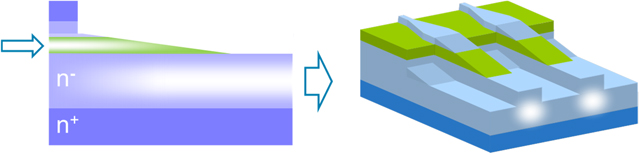
Figure 13. Left: cross-section of a vertically tapered spot-size converter illustrating how the mode of the upper waveguide is coupled to a waveguide with a larger mode diameter. Right: 3D picture illustrating how the SSCs can be integrated in dense arrays.
Download figure:
Standard image High-resolution imageThe COBRA SSC has 0.5–1 dB coupling loss to a lensed fibre or an interposer chip with 3 μm spot diameter and it has a small pitch (25 μm), which makes it suitable for integration in dense arrays [55]. It is not yet available in MPW runs.
Concentrating the SSCs in dense arrays, e.g. for switching matrices, is useful for reducing the chip area occupied by the SSCs. For such dense arrays an interposer chip of dielectric waveguide material is required to couple the signals out of the chip, as fibre diameters are too large to match a 25 μm pitch. The interposer can be used to adapt the pitch of the SSC-array to that of a fibre array, but it may also contain passive devices like delay lines and high-Q filters with much better performance as offered by the InP chip because of the much lower losses of dielectric waveguide platforms (<0.1 dB). In this way it may serve as a hybrid platform, combining the best of InP and dielectric waveguide technology, and the dense SSC array serves as an optical bus between the two chips. The JePPIX partners are cooperating with the Dutch company LioniX to develop such a hybrid platform technology.
Other Platforms. HHI provides an SSC with a similar structure to that introduced above, which adapts the Mode Field Diameter (MFD) to that of a cleaved Standard Single Mode Fibre (SSMF, MFD = 9 μm). The coupling loss is 1.5–2 dB and the minimum pitch is 25 μm. In the Oclaro platform, selective area epitaxy is employed to expand the mode size and make it circular with a diameter of 3 μm. A coupling loss of 0.5 dB to a lensed fibre with an MFD of 3 μm is specified. Oclaro allows SSCs to be flexibly spaced with a minimum separation of 500 μm.
COBRA is presently working on an SSC which avoids the vertical tapering by using lateral tapering of the upper waveguide to push the mode down to the FMW. If the lateral taper is written in the same lithography step as the waveguides this leads to a reduction of the number of process steps. It requires a high resolution and dimensional control of the lithography, which is feasible with DUV lithography.
5. CBBs
A CBB is any combination of two or more BBBs. Whether we call such a combination a CBB or not depends on its potential for re-use: if it can be re-used as a building block in a more complex circuit it is a CBB. So MMI-couplers and AWGs are CBBs, but also more complex sub-circuits like a full DQPSK receiver can be a CBB if it is used as a building block in a more complex ASPIC. CBBs can be parameterized: in a WDM transmitter consisting of a set of DBR lasers and an AWG for multiplexing the WDM signals, the DBR laser is a CBB. But to avoid that we end up with a separate CBB for every wavelength we can enter the emission wavelength of the DBR laser (determined by the period of the DBR grating) as a parameter, so that we can build a full DBR laser array with a single CBB. And for an AWG, for example, we may enter the central wavelength, the channel spacing, the FSR and the bandpass shape as a parameter.
A CBB can be re-used by a designer in his own ASPIC. But it is much more useful if it is stored in a component library so that every designer who has a licence for that library, can use it. The most important modules to be stored in a CBB-library are a mask layout generation module and a simulation module which the designer can use in a circuit simulator. CBB libraries are usually part of the PDK which is provided by the foundries or a broker to designers that want to participate in an MPW run. The application potential of a foundry process is, to a great extent, determined by the number and the quality of the CBB-modules that are available in the library. Building an extensive CBB-library is a major task and a continuing effort for developers and users of a foundry process, which will lead to a steady increase of the application potential of the process.
Below we will briefly describe the most frequently used CBBs.
5.1. Junctions between different waveguides
Any ASPIC will have different types of waveguide, straight and curved, shallow and deep etched, active and passive, and waveguides with different widths. Each waveguide has its own mode-profile, and some of them can carry several modes. If we just connect them we will introduce coupling loss and back reflections at the junction. For maximal coupling and minimal back reflection the junctions have to be carefully designed.
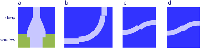
Figure 14. Junctions between different types of waveguides: (a) shallow and deep etched waveguides; (b) straight and curved waveguides; (c) curved waveguides with opposite curvature; (d) same as (c) but with angled facets for low reflectivity.
Download figure:
Standard image High-resolution imageThe junctions described below do not incur additional process complexity, they can be realized by the designers using standard BBBs or, as in the case of deep to shallow waveguide matching elements, be offered by the platforms as CBBs using the same basic process sequence. They can have physical dimensions, but some of them consist just of an offset between two waveguides, which is optimized to reduce the junction losses. If properly designed, junction losses will be small (typically lower than 0.1 dB) and reflections low (<−40 dB). For accurate designs their properties, like transmission loss, back reflection and mode conversion (including coupling to radiation modes) should be accounted for in the circuit simulation. The most important junctions are the following:
- Shallow-deep junctions Figure 14(a) shows a top view of a low-loss junction between shallow and deep waveguides. At the junction the deep etched waveguide is a bit wider than the shallow one in order to get an optimal match between the mode profiles in both waveguides. Further, the wider waveguide section is extended a few μm into the shallow region to avoid the possibility of a deep slit occurring between the deep and shallow etched waveguide due to a small mask misalignment. The junction is followed by a taper because the standard deep etched waveguides are narrower than the shallow etched ones. For minimal reflection the interfaces should be angled.
- Straight–curved and curved–curved junctions Junctions between straight and curved waveguides are shown in figure 14(b). Here an offset and a width adjustment are applied to get an optimal match between the mode profiles in the straight and the curved waveguide, where the mode shifts to the outer edge and is slightly compressed. Junctions between curved waveguides with opposite curvature (figure 14(c)) have an offset which is approximately twice the offset between a curved and a straight waveguide. The abrupt offsets as depicted in (b) and (c) may cause small reflections. These can be reduced by applying angled facets as shown in figure 14(d). They will have negligible effect on the transmission, but lead to a significant reduction of the back reflection.Another way of reducing back reflection is to apply a slow change of the curvature (approximating an adiabatic transition). This can also reduce the small amount of mode conversion that occurs at an abrupt junction, but at the cost of a significantly larger length of the total bend.
- Active–passive junctions Whereas the junctions between passive waveguides offer the designer some design freedom, the design of junctions between active and passive waveguide sections is usually fully determined by the process developer (the foundry). For accurate design their physical properties, such as coupling loss, back reflections, mode conversion and radiation have to be included in the modelling. Back reflections play an important role, especially in circuits with a high gain, where they will lead to fringes in the wavelength response, and at high gain values they may cause poor side mode suppression or even lasing at undesired wavelengths. For good junctions back reflections are below -40 dB. Even at this level they can have visible effects, however.
- Tapers between waveguides with different widths In order to avoid mode mismatch loss and back reflections a taper is used to connect two waveguides with different width. The loss can be very low, if the taper angle is chosen sufficiently small (adiabatic tapering). Taper length increases quadratic with the width. For large taper ratios a parabolic tapering profile is, therefore, optimal. For small taper ratios a linear taper is adequate. A taper from a 2 to 3 μm wide shallow waveguide requires a length of about 50 μm, tapering from 2 to 1.5 μm requires about 20 μm.
5.2. MMI-components
5.2.1. MMI-couplers
Combining and splitting of signal power are basic functions in almost any circuit. It can be done with star couplers, directional couplers or MMI-couplers. Star couplers are good for high splitting ratios, but they have significant non-uniformity and splitting loss. Directional couplers can have very low insertion loss and back reflections, but in high-contrast waveguide technology the gap between the waveguides needs to be submicron and it is difficult to control the coupling ratio accurately. MMI-couplers [56, 57] are, therefore, the most frequently used couplers.
An MMI coupler is a multimode waveguide section in which single or multiple copies of the field at the input facet are imaged on the output facet. The imaging is based on decomposition of the input field into the modes of the MM-section and reconstruction of single or multiple images at certain lengths, where all the modes arrive with the proper phase. The imaging properties are dependent on the MMI-section length and the position and shape of the input and output waveguides. Figure 15 shows the schematic layout of MMI-couplers used as (a) 1 × 2 power splitters or combiners and (b) 2 × 2 couplers. They can be realized both in shallow and deep waveguide technology. The imaging quality, and hence the insertion loss and the cross-talk are better for a deep etched MMI-section, but the reflections at the end faces are lower for a shallow etched coupler. MMI-couplers with deep etched sidewalls and shallow etched end faces (as shown in figure 15), combine both advantages. Further reduction of reflections can be achieved by applying angled facets [58] as indicated in figure 15(c) or even more sophisticated shapes of the end facets [59]. They prevent that light reflected at the end facet can couple back to the input port.
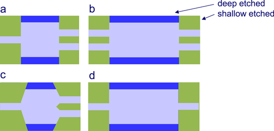
Figure 15. Multimode interference (MMI) couplers and filters: (a) 1 × 2 power splitter or combiner (b) 3 dB coupler (c) MMI-coupler with angled facets for reducing end facet reflections (d) first-order mode filter.
Download figure:
Standard image High-resolution image5.2.2. MMI-filters
MMI-couplers with one input and one output port, as depicted in figure 15(d), can be used as mode filters [60]. When properly designed they transmit the fundamental mode and suppress the first order mode, which can be excited at asymmetrical junctions in the waveguide or by reflection at angled facets.
5.2.3. MMI-reflectors
On-chip reflectors are important components for flexible design of FP cavities (e.g. in lasers), because they can be placed everywhere on the chip. This avoids the need of positioning the cavity at a cleaved end face and it also allows better control of the dimensions of the cavity. Further, on-chip reflectors allow for on-wafer testing of devices, because the wafer need not be cleaved in order to obtain the laser mirrors. The most commonly used way to fabricate on-chip reflectors is by using DBR or DFB gratings. This requires high-resolution lithography, either DUV, holographic or E-beam. A simple way to realize a reflector in a shallow-deep etching process is by providing a 1 × 2 MMI coupler with a corner mirror at the end facet for obtaining total reflection, as depicted in figure 16 (left). The corner mirror consists of two deep etched (totally reflecting) 45° mirror facets. The two images will be reflected by the two mirrors, which work as a corner reflector, and focused back on the input waveguide. The component can be considered as a folded 1 × 1 coupler with twice the length of the 1 × 2 coupler, in which the folding line is replaced by a corner mirror. In this way mirrors with less than 1 dB reflection loss can be realized. We call them multimode interference reflectors (MIRs). If two waveguides are connected at the input, the signal coupled into one input is reflected back into both waveguides, as depicted in figure 16 (middle), so that the component works as a partially transmitting mirror. By folding 2 × 2 couplers or asymmetric MMI-couplers 50/50 and 85/15 transmission and reflection ratios can be obtained, and with tapered MMI-couplers any desired ratio can be realized in principle [61]. A distinct advantage of MIRs is their broad spectral width compared with DBR mirrors.
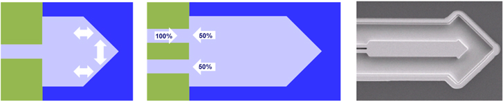
Figure 16. MMI-reflector with total reflection (left) and partial reflection and transmission (middle). Right a SEM photograph of a MIR with a reflection and a transmission port, surrounded by a deep trench. The MIR shown in the photograph has no shallow input waveguides.
Download figure:
Standard image High-resolution image5.3. AWG (de)multiplexers and routers
Arrayed Waveguide Gratings or PHASARs, as they were called in the early days, are widely applied as wavelength (de)multiplexers, routers and filters [62]. AWGs have been reported with both shallow and deep etched waveguides. Shallow etched AWGs can have losses below 2 dB, but they are rather large (several mm) because of the large bending radii in the waveguide array. Deep etched AWGs can be much smaller, but have larger losses (typically >5 dB). The losses occur at the junction between the waveguide array and the free propagation regions (FPR), as shown in figure 17 (left). For low loss, the gaps between the array waveguides close to the FPR should be very sharp so that the guided modes in the array will couple adiabatically to the slab waves in the FPR and vice versa. Due to the characteristics of the etch process and the finite lithographic resolution the gaps will close abruptly, however, which causes a discontinuity that will introduce scattering and reflection losses. Because of the high contrast these losses can easily exceed a few dB per junction. A solution to that problem is the application of combined deep and shallow etched waveguides [63], as depicted in figure 17 (middle). Both the array waveguides and the receiver and transmitter waveguides are deep etched, which leads to very small array dimensions: 330 × 230 μm for the 4-channel device shown in the figure. The deep etched region can be seen in the figure as the complex shaped box around the AWG. Figure 17 (right) shows a SEM-picture of the junctions between the FPR and the waveguide array, and between the shallow and deep etched waveguides. The closing of the gaps is clearly seen. Because the discontinuity occurs in the shallow etched region it brings a much lower loss. The tapered junctions from shallow to deep waveguides, as schematically depicted in figure 14(a), can also be seen in the SEM-picture. Using DUV lithography the closing of the gaps occurs at much smaller gap widths and using DUV-lithography, low-loss AWGs should be feasible with deep etched waveguides only.
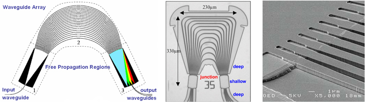
Figure 17. Left: schematic picture of an AWG demultiplexer. Middle: compact 4-channel AWG with combined shallow and deep etched waveguides. Right: SEM picture of the region around the junction between the waveguide array and the FPR, showing the closing of the gaps and the tapered shallow-deep waveguide junctions.
Download figure:
Standard image High-resolution imageIn AWG-design, a large variety of device specifications is possible: number of input and output ports, channel spacing, FSR, bandpass shape (parabolic or flattened), just to mention the most important ones. The most practical way to cover this variation in AWG design is by using a number of different library modules (see section 7 below for a more extensive description of how design libraries can be used in the platforms). By parameterizing the module so that it can handle designs with different channel spacings, FSRs and possibly also different numbers of input and output ports, the number of modules required for the most common operations may be reduced to a few. The current AWG libraries cover parameterized designs.
5.4. FP-lasers and ring lasers
The first semiconductor lasers were FP lasers. They were realized by fabricating an array of active SOA waveguides on a wafer, cleaving the wafer into bars, and cleaving the bars into individual laser chips. The cleaved facets were used as reflectors, without coatings they have a reflectivity in the order of 30%. The length of the cavity was determined by the cleaving of the bars. FP lasers are typically multimode lasers, they will lase at a number of longitudinal cavity modes simultaneously. The modes are spaced by the so-called FSR, which is determined by the length of the FP-cavity. Recently FP lasers were used as building block in single-mode lasers. In these lasers the FP-laser is forced to operate in a single FP-mode using filtered feedback [64]. The FSR is matched to the ITU wavelength grid, so that the cavity length needs to be controlled very accurately. This is not possible with cleaving. Figure 18 (left) show a schematic and a SEM-photograph of an FP laser which has been formed by using MIRs as broadband reflectors instead of the cleaved facets. In this way the cavity length can be controlled much more accurately. A way to form a laser without reflectors is by using a ring cavity, as shown in figure 18 (right).
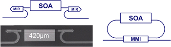
Figure 18. Left: schematic and SEM photograph of a Fabry–Perot laser formed by a SOA section integrated between two broadband MIR reflectors. The waveguides are embedded in a deep etched trench. Right: schematic of a ring laser.
Download figure:
Standard image High-resolution image5.5. DBR and DFB-lasers
Another and more common way to make lasers single-mode is by using gratings as wavelength selective reflectors. If we replace the two MIRs in figure 18 with gratings, we get a DBR laser. If we use the tunable gratings that are provided on the Oclaro platform we get a tunable DBR laser. The standard gratings provided in the Oclaro platform can be tuned by current injection to give a change in effective refractive index in the region of −0.022, sufficient to tune the laser over approximately 10 nm in the 1550 nm wavelength band. By optimizing the reflectivity of the front and rear-gratings (choosing a proper grating length) and by including a phase shifter in the cavity, a tuning range of 5–8 nm can typically be realized, while maintaining single frequency operation with high side-mode suppression ratio (SMSR) [74]. For larger tuning ranges more sophisticated designs are required, e.g. [76].
In DFB lasers, as opposed to DBR lasers, the reflecting grating is incorporated into the gain section itself by placing it above or beneath the active region, or at the sidewalls. In the present versions of the platforms this option is not available. HHI is working, however, on incorporating it in a future release of its foundry platform.
5.6. MZI and MI-modulators
An amplitude modulator or a space switch can be obtained by putting one or two phase modulators in the branches of a MZI Modulator, formed by two MMI-couplers. By applying 180° phase shift in one of the arms, the input signal can be switched from the cross-port to the bar port. Figure 19 shows a schematic and a typical switching curve of a MZI modulator, which can also be used as a space switch. Switching voltages at 1550 nm are between 3 and 4 V for a 1 mm long electrode in the Oclaro platform, and around 7 V for a 2 mm long electrode in the COBRA platform. The switching voltage is both polarization and wavelength dependent. The electrode length and the capacitance can be reduced by a factor of two by using the phase modulators, combined with a reflecting element (cleaved facet or MMI reflector), in a Michelson interferometer configuration, as described in [78].
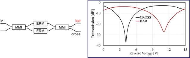
Figure 19. Left: Schematic of a Mach–Zehnder and (right) switching curve of a Mach–Zehnder with 2 mm long electrode.
Download figure:
Standard image High-resolution imageThe CBBs discussed above are only a few of the most important building blocks. Many other CBBs like DQPSK receivers, switch matrices and complex lasers can be fabricated on the generic platforms and will be investigated and included in the component libraries.
6. ASPIC examples
In this section we give some examples of Application Specific Photonic ICs (ASPICs) that have been realized in the generic foundry processes of COBRA, Oclaro and the Fraunhofer HHI. Most of the examples have been developed in the framework of the EuroPIC [39] and PARADIGM [40] projects, and some of them in two Dutch national projects: MEMPHIS [41] and the IOP Photonic Devices [42]. Access to MPW runs in the InP foundry processes is offered by the JePPIX platform (www.jeppix.eu).
6.1. COBRA platform
COBRA has been pioneering with the development of generic integration processes since the beginning of the century [37]. Since 2007 it has provided access to its generic integration process for research purposes to external partners, in the framework of the JePPIX platform [44]. In 2013 COBRA-spinoff SMART Photonics began offering (semi-) commercial access to this platform, while COBRA is working on many extensions to the capabilities of InP-based generic integration technology as described in the previous sections. Below some examples are given of chips realised in the COBRA process.
Fast discretely tunable laser. Figure 20(a) shows an AWG-based discretely tunable laser with nanosecond switching speed based on a novel concept [65]. It uses a booster amplifier in the common waveguide of the AWG and short SOA gate switches in the waveguides connected to the demultiplexed side of the AWG. These short SOAs can be switched within a few ns with currents as low as 1 mA. Laser peaks have side mode suppression ratios of 30–40 dB. The switching between AWG channels is discrete and no laser operation takes place at wavelengths corresponding to other channels during the tuning process (dark tuning). This makes the device promising for packet routing and switching applications.

Figure 20. Examples of Photonic ICs realised on the generic COBRA platform. (a) AWG-based discretely tunable laser with nanosecond switching speed (1.5 × 3.5 mm2); (b) 320 Gb s−1 monolithic multistage SOA switching circuit, (c) multifunctional delay interferometer (4 × 2 mm2); (d) 4 × 4 space and wavelength selective cross-connect (4.2 × 3.6 mm2); (e) monolithic 16 × 16 photonic switch for broadband photonic packet-routing (4.0 × 13.2 mm2); (f) broad frequency comb laser (0.3 × 2.2 mm2).
Download figure:
Standard image High-resolution image320 Gb s−1 switching matrix. Figure 20(b) shows a multi-stage interconnection chip with nanosecond reconfigurability and a demonstrated capability of routing 320 Gbit s−1 line-rate signals [66, 67]. The chip comprises twelve pairs of SOA gate switch elements which are wire bonded to a ceramic carrier. Two pairs of SOA gates form a cross-bar switch CBB. Six such building blocks are then implemented to connect four input ports with four output ports in a four stage network. All of the input and output waveguides are accessed via the front facet of the chip and placed at a pitch of 250 μm for packaging compliance. This is the first active-passive multistage circuit reported.
Multi-functional delay interferometer. Figure 20(c) shows a chip which can perform the following functions: optical buffering, differential phase-shift keying (DPSK) demodulation, intensity modulation, and differential XOR logic operation [68]. By properly controlling the current supplied to the active elements in the circuit loop (i.e. a SOA and a variable optical attenuator), the relative phase of the propagating signals can be adjusted, changing the interference condition between the input signal and its delayed copies. In buffer configuration, up to 13 circulations (corresponding to a 1.62 ns delay for 12.5 Gb s−1 data) are demonstrated. Used as DPSK demodulator no significant BER power penalty is observed for 8 Gb s−1 signals, compared to a thermally tuned commercial demodulator. Error-free operation for a 1-, 2-, and 4-bit differential XOR logic gate has been demonstrated at 8, 16, and 32 Gb s−1, respectively.
4 × 4 space and wavelength-selective switch. Figure 20(d) shows a four input four output space and wavelength selective cross-connect [69]. The circuit is implemented with 32 SOA gate switches and four cyclic 4 × 4 AWG routers with a nominal 400 GHz wavelength channel spacing. This allows for the arbitrary and fast reconfigurable connection of wavelength channels from each input to each output. The circuit is the first in class for simultaneous wavelength and space selective routing. Multi-path routing was performed with both co- and counter-propagating data. Bi-directional and fast reconfigurable routing has similarly been quantified to show low power penalty of less than 1 dB for the simultaneous routing of data over multiple circuit paths.
16 × 16 photonic switch. Figure 20(e) shows a monolithic sixteen input, sixteen output photonic switch which is designed for broadband photonic packet-routing [32, 70]. The circuit is constructed as a hybrid Beneš architecture in three stages, with arrays of 2 × 2 switch building blocks at the inputs and outputs, and a centre stage implemented with an array of eight 4 × 4 switch building blocks. Switching within each of the building blocks is implemented by broadcast and select: The broadcast is facilitated with 288 multimode interference (MMI) splitters, and the select function is implemented with 192 SOA gates. With a total of 480 components integrated on a single chip this is one of the largest PICs reported so far. The use of low loss passive waveguides in combination with high contrast active gates leads to promising system level metrics in terms of optical signal to noise ratio and electrical energy use [32]. Multi-path dynamic reconfiguration is enabled through the connection of the circuit to programmable logic [70].
Broad frequency comb laser. Figure 20(f) shows a mode-locked ring laser with a very wide comb spectrum [71]. The laser consists of straight and curved waveguides, an SOA section, a saturable absorption element, electrical isolation sections and a 2 × 2 MMI coupler. The SOA element, which provides optical gain, was divided into two sections of equal length (345 μm) with a 30 μm long saturable absorber in between. For the SA a short reverse biased SOA section was used. The laser was operated by reverse biasing the SA and forward biasing the SOA sections. It features a 20 GHz comb spectrum with FWHM bandwidth of 11.5 nm (1.41 THz) and 17 nm (2.16 THz) when measured at -10 dB. These are record values when compared to the results obtained from devices with a similar geometry based on QW material.
6.2. Oclaro platform
Oclaro has been involved from the beginning in the ePIXnet initiative for the introduction of a foundry model into photonic integration. It is participating in the JePPIX platform. For its commercial products Oclaro has developed a technology for integration of tunable DBR-lasers with MZI modulators [72]. This technology offers high performance SOAs, tunable DBR gratings and phase modulators. In the EuroPIC project Oclaro worked on preparing this technology to support a broad range of functionalities in both telecom and non-telecom applications. In the PARADIGM project it is working on further extension of its capabilities to 40 Gb s−1 full transmit and receive functionality. Below a number of examples are given of experimental ASPICs that have been realized in Oclaro's first generation generic platform technology. The chips have been developed in the framework of the EuroPIC project and the Dutch MEMPHIS project.
Low energy scalable high speed optical switch. Figure 21(a) shows a chip containing 2 × 2 port building blocks for an ultra-low energy scalable high speed optical switch [73]. This device comprises both Mach–Zehnder modulators and SOAs to optimize switching energy and performance in nanosecond switching time lossless switches for data centre and internet switching and routing applications. The component has very low power penalty. After three cascades which would emulate an 8 × 8 port switch, the eye diagram shows almost no impairment. Input power dynamic range is 14 dB for a 0.5 dB penalty. The switch does not require 50 Ω matching resistors which dramatically reduces its electrical power consumption. This is all predicted to result in a 95% power reduction compared to a conventional SOA switch.
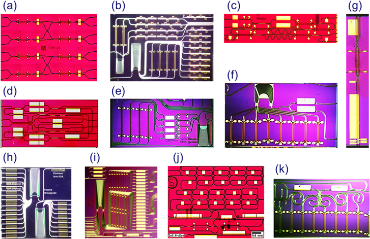
Figure 21. Examples of photonic ICs realised on the generic Oclaro platform. (a) Low energy optical switch; (b) PIC with a 4- and an 8-channel WDM transmitter. The 8-channel transmitter integrates 74 components on a chip area of 3 × 5 mm2; (c) a 1 × 4 mm2 InP 'all optical' transmultiplexer chip; (d) widely tunable laser chip; (e) filtered-feedback multi-wavelength transmitter (2 × 4 mm2); (f) 8-channel WDM reflective modulator with dimensions 3 × 2 mm2; (g) pulse laser with tunable repetition rate; (h) AWG-based multiwavelength laser used for TeraHertz generation by mixing of two channels; (i) pulse shaper for bio-imaging integrating a 20-channel AWG with 20 SOAs and 20 phase modulators. The chip measures 6 × 6 mm2; (j) 10 bits switched delay line. The chip measures 4 × 6 mm2; (k) 8-channel pulse serialiser containing 2 SOAs, 8 MI-modulators and 7 delay lines.
Download figure:
Standard image High-resolution imageWDM transmitter. Figure 21(b) shows a WDM transmitter for use in the Central Office of a FTTH network [74]. The transmitter chip contains an array of DBR-based lasers and Mach–Zehnder modulators. It is designed for transmitting four modulated downstream (DS) data channels and four CW signals on which the upstream data can be modulated at the subscriber using a reflective modulator. An AWG is used to multiplex all the optical signals into one common output waveguide. The transmitter is designed to operate at a 100 GHz wavelength grid at 1550 nm. It delivers up to 4 dBm of optical power/channel into the fibre with a modulation data rate of 12.5 Gbps per channel.
WDM-TDM transmultiplexer. Figure 21(c) shows the first integrated all-optical WDM-TDM multiplexer, for wavelength grooming of a number of WDM channels into a single TDM channel at the aggregate line rate [75]. For design and mask layout of the Mux circuits, simple equivalent circuits were developed, representing the incorporated wavelength converter. With the realized chips, successful WDM to TDM transmultiplexing was demonstrated from 2 × 10 Gb s−1 WDM to 1 × 20 Gb s−1 TDM, as well as multiplexing of clock and NRZ data to narrow pulse RZ data.
Widely tunable laser. Figure 21(d) shows a new widely and continuously tunable ring laser [76]. The chip combines two gain sections with an integrated, tunable 4th order series filter with a Vernier pair of ring resonators (RR) and a pair of identical delayed interferometers (DI). With an identical and optimized phase shifter (in forward bias: ~90° mA−1) in all RRs and DIs, tuning currents of only a few mA yield tuning ranges of 2000 GHz. Vernier pairing of the DIs doubles this continuous tuning range to 4000 GHz.
Filtered-feedback multi-wavelength transmitter. Figure 21(e) shows a filtered-feedback multi-wavelength transmitter [77]. The laser consists of an array of FP lasers, each of which is formed by a SOA and two on-chip broadband MMI Reflectors (MIRs). One side of each FP laser is coupled to an AWG filter through a phase shifter. The AWG acts as a wavelength filter outside the laser cavity, and its output port is connected to another MIR to provide feedback. The phase shifting sections can adjust the phase of the feedback signal to optimize the stability of the laser. This laser can operate with four channels simultaneously. Each channel has stable single mode lasing with an SMSR better than 40 dB. The filtered feedback reduces the laser linewidth to 150 kHz. The outputs of the laser channels are routed to 1 mm long MZ modulators on the same chip.
8-channel WDM reflective modulator. Figure 21(f) shows an 8-channel WDM reflective modulator using Michelson-interferometer modulators [78]. Measured bandwidth of the Michelson modulators is >18 GHz. Eye-diagrams for 12.5 Gb s−1 signals in back-to-back configuration are wide open with a dynamic extinction ratio of 10 dB. Transmission experiments through 85 km of SMF fibre showed error-free operation at 10 Gb s−1.
Pulse laser with tunable repetition rate. Figure 21(g) shows a mode-locked pulse laser operating at 14.4 GHz monolithically integrated with a pulse-picking Mach–Zehnder modulator for reducing the pulse rate and an SOA for increasing the output power [79]. The laser generates 12.5 ps pulses. The Mach–Zehnder modulator allows tunable repetition rates from 14 GHz to 109 MHz, and the SOA boosts the peak power by 3.2 dB. The device approaches performance figures suitable for biophotonic applications in a compact and cost effective platform.
Dual wavelength laser for THz generation. Figure 21(h) shows an AWG-based multi-wavelength laser which is used for generation of a 95 GHz carrier frequency by optical heterodyning of two wavelengths from adjacent channels of the AWG-laser. The extended cavity structure of the device provides low phase noise and narrow optical linewidth, further enhanced by the intracavity filter effect of the arrayed waveguide grating. The generated RF beat note, at 95 GHz, has a −3 dB linewidth of 250 kHz. This is the narrowest RF linewidth generated from a free-running dual-wavelength semiconductor laser [80].
Pulse shaper for bio-imaging. Figure 21(i) shows an integrated pulse shaper with a reflective geometry [81]. The PIC combines a 20-channel AWG-filter with 50 GHz channel spacing, 20 electro-refractive phase modulators (ERMs) and 20 SOAs. The light from the optical pulse source, i.e. a mode-locked laser, is divided into twenty spectral components by the AWG. The ERMs and SOAs are used to manipulate the spectral phase and amplitude of the components in order to achieve the desired pulse shape. The spectral components are then recombined in the AWG. The integrated pulse shaper is used to demonstrate chirp compensation for the pulses from a mode-locked quantum dash laser diode. Reduction of the pulse width from 7 ps to less than 3 ps is demonstrated.
Ten-bit switched delay line. Figure 21(j) shows a photonic 10 bits switched delay-line circuit for use in a BOTDR strain sensor system [82]. The circuit consists of a chain of delay elements. In each delay element light is split over two optical paths by an MMI-splitter. Each path contains an SOA that can be operated as a gate switch: either blocking or amplifying the light. By controlling the SOAs light can be selected from either the longer or the shorter path of the delay element. The optical path of the whole chain consists of 10 switchable delaying elements with length ratios 1, 2, 4, ..., 512 and it can be tuned over 1024 different delay values.
8-channel pulse serialiser. Figure 21 shows an 8-channel integrated photonic pulse serialiser with dimensions 3 × 2 mm2 [83]. The chip is designed as a data read-out unit for the KM3NeT Neutrino Telescope which is planned to have 186 000 Photo-Multiplier Tubes that have to be read out every nanosecond. The ASPIC architecture consists of a distribution network with 1 × 2 MMI power splitters and optical delay lines for multiplexing of optical pulses in the time domain, SOAs for loss compensation and reflective amplitude modulators in MI configuration for data encoding. A static extinction ratio of over 12 dB was measured. The distribution network provides accurate time delay and multiplexing of the 1 Gb s−1 readout signals on a 32 Gb s−1 output frame.
6.3. Fraunhofer HHI platform
Fraunhofer HHI has developed a technology for fabrication of high speed receivers, the key element of which is a high-speed waveguide integrated pin photodiode [84]. It is commercially exploited by u2t Photonics (www.u2t.com), a spin-off company of HHI. This technology offers high performance balanced detectors and their integration with passive components and SSCs. In the EuroPIC project HHI has been working on preparing this technology for supporting a broader range of applications in a foundry setting. In PARADIGM it is working on further extension of its capabilities to full 25 Gb s−1 transmit (Tx) and 40 Gb s−1 receive (Rx) functionality. Below a number of examples are given of experimental ASPICs that have been realized in HHI's generic platform technology. The chip shown in figure 22(e) has been realized on the new Tx/Rx platform.

Figure 22. Examples of Photonic ICs realised on the generic Fraunhofer HHI platform. (a) Frequency discriminator chip containing MZI structures coupled with ring filters and balanced photodiodes; (b) integrated QPSK receiver chip; (c) opto-rf converter for sub-THz applications; (d) read-out chip for a 4-channel FBG strain sensor; (e) transmitter for cw THz applications implemented on HHI's extended Tx/Rx integration platform.
Download figure:
Standard image High-resolution imageIntegrated frequency discriminator. Figure 22(a) shows an integrated frequency discriminator for application in phase-modulated microwave photonic links [85]. It contains a cascaded structure of lattice filters realized by ring-loaded MZIs to result in an IIR-equivalent optical filter. An input filter splits the spectrum of the FM optical signal into two separate bands each of which is fed into a filter providing a linear ramp in intensity. Finally, both bands are detected in a balanced detector. Comparison of experimental and simulated filter characteristics already indicates good agreement for this first fabrication run. The discriminator exhibits SFDR values between 67 and 79 dB.Hz2/3 for signal frequencies in the range of 5–9 GHz, basically limited by the experimental test setup. We expect that values in the range of 104–116 dB.Hz2/3 will be achievable.
Integrated QPSK receiver. Figure 22(b) shows a receiver chip for the detection of 28 Gbaud QPSK transmission signals [86]. Its central element is the 90° hybrid mixer implemented in the form of a 2 × 4 MMI coupler. This coupler is connected to two pairs of waveguide-integrated dual photodiodes for the I and Q channels. Waveguide crossings are used in the output network to fulfil the phase relationship between the neighbouring diodes. The input waveguides provide mode expansion (SSC) enabling coupling loss as low as 1 dB to SSM fibres. Responsivity of the device shown is close to 0.1 A W−1 over the C-band, with CMRR values of −10 dB in the worst case.
Opto-rf converter for sub-THz generation. Figure 22(c) shows an integrated chip that comprises a high-frequency photodiode coupled with a logarithmic periodic antenna [87]. The photodiode itself can be remotely biased by three other photodiodes connected in series with it and optically powered via the input fibre and an on-chip 1:4 MMI power splitter, thus avoiding any external electrical biasing. The antenna converts high-frequency optical signals into microwave/sub-THz radiation. Launching light from a tunable heterodyne laser source into the device, radiated power in the 1-digit μW range at around 5 mA of photocurrent was obtained in the frequency range up to 400 GHz.
Read-out chip for 4-channel FBG strain sensor. Figure 22(d) shows two wavelength metres on a chip with fibre matched SSCs. The devices measure a wavelength shift in a fibre Bragg grating, anywhere in the 1465–1620 nm window [88]. Each device has a 1 × 2 MZI and the signals from the outputs of the 2 × 2 MMI in each MZI are fed into a balanced detector. The wavelength metres have a FSR of 10 pm and 100 pm, using an integrated spiral delay line with 64 mm length for the 10 pm FSR. The responsivity of a packaged device is 0.29 A W−1. A subfemtometer resolution is feasible at a sampling rate of 10 kHz and −10 dBm fibre power. This is several orders of magnitude better than commercially available small-sized wavelength metres.
Transmitter for THz applications. Figure 22(e) shows a PIC designed for continuous wave THz generation [89], which has been fabricated during trials of the new HHI Tx/Rx platform. Two wavelength-tunable DFB lasers are incorporated into an MZI structure together with current injection based optical phase modulators and MMI couplers. This chip provides full control of the THz signal by using a unique bidirectional operation technique. Integrated heaters on the laser elements allow for continuous tuning of the THz frequency over 570 GHz. Applied to a coherent cw THz photomixing system operated at 1.5 μm optical wavelength, a signal-to-noise ratio of 44 dB at 1.25 THz was reached, which is identical to the performance of a standard system based on discrete components.
7. ASPIC design environment
The introduction of the generic foundry approach in photonics will cause a major change in the sophistication of photonic chips: it will move the design from a device level to a circuit level, a move that occurred in microelectronics in the 1970s and 1980s, and that is now happening in photonics too.
In the generic approach a high performance standardized process is accessible via PDKs with a number of building blocks, the performance and functional behaviour of which is accurately known. Designers do not have to be concerned about how to design them, they can just take them from a library and start building a circuit and analyse and optimize it with a circuit simulator. Of course a good knowledge about the operation of the building blocks is still important, but detailed knowledge about the process technology and the layer stack is no longer required. Therefore the designer can concentrate on a higher abstraction level of circuit design. Just like system designers that build their circuits from discrete optical components, of which they know the behaviour, but not what's exactly inside the box. ASPIC design is very similar, but now the system is integrated on a single chip. Further the designers have some additional freedom because a number of the building blocks are parameterized, so that they can adapt their performance to specific requirements, which is not so easy with discrete components, where only a limited number of different types will be available.
We will briefly describe what the Design Environment for a generic process looks like.
7.1. Software environment
The Software Environment contains the required software tools; these include not just circuit simulators and mask layout tools, but also physical modelling tools such as mode-solvers, BPM, EME or FDTD tools, nonlinear time domain models, electrical and thermal simulators. All or any of which may be required for performing simulations on a sub-circuit or device level.
7.1.1. Circuit simulators
Circuit simulators sit one level above physical simulators. They make the assumption that the light is flowing in clearly defined waveguide modes. This allows them to simulate much larger devices than a physical simulator could. Circuit simulators work with surrogate models of the actual components making up the circuit—i.e. models that give the correct behaviour (within defined limits) but using simplified mathematical models that can be evaluated quickly.
Within the EuroPIC [39] and PARADIGM [40] consortia three circuit simulators are used: Aspic™ from Filarete for linear wavelength domain simulations, PICWave from Photon Design for nonlinear time domain simulations and ADS, Agilent's Advanced Design System for optical, RF, microwave and high speed digital applications. ADS offers a very powerful simulation and parameter extraction engine, which is not (yet) commercially supported for photonic design, however. We will give three examples of circuit simulations that illustrate their potential for Photonic IC design on the JePPIX InP platforms.
7.1.2. Aspic™ (Filarete)
Aspic™, Advanced Simulator for Photonic Integrated Circuits [90], is a frequency domain circuit simulator for passive linear PICs. Each building block is described by analytical models and numerical data embedded in scattering matrices. Models can be either derived from the theoretical behaviour of the building blocks or can be built through electromagnetic simulations, and can also include experimental data. Foundry based models containing the realistic description of building blocks fabricated by several photonic foundries (e.g. Oclaro, HHI, COBRA/SMART for InP technology) are available and organized into specific libraries.
Arbitrarily complex PICs can be designed by combining a large number of basic and composite BBs included in the BB libraries. To perform the simulation, Aspic™ assembles the scattering matrices of all the BBs of the circuit and provides amplitude, phase, group delay response, and chromatic dispersion at the input/output port of each BB (forward and backward field). Scan and sweep operations versus any geometrical or optical parameter of the circuit can be performed as well. Once the circuit is optimized by the user, it can be directly exported to a mask layout editor (MaskEngineer).
Large flexibility in the choice of the BB parameters makes the user do much more than a simple spectral analysis, enabling for instance 'what if' analysis, virtual experiments, tolerance analysis, case analysis, statistical analysis based on Monte-Carlo simulations to evaluate the robustness of the circuit against fabrication uncertainties, and so on. Figure 23 shows a typical screen shot of the simulator. It shows a discretely tunable delay line used in one of the ASPICS discussed in the previous section [82]. It is based on a split and select technique with SOA gates. The state of each SOA is defined by its electrical current, which is loaded from a text file, and the spectral response is simulated for each state. The output power and the group delay at a given wavelength are shown in the plot below. The simulation of this rather big circuit requires just a few seconds to be performed, a result not achievable with electromagnetic simulations.
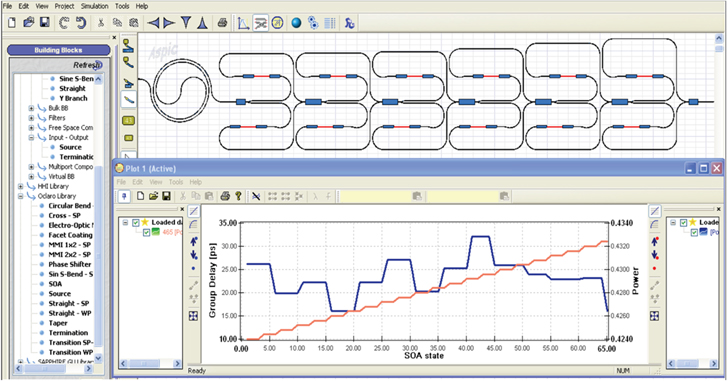
Figure 23. Screenshot of the Aspic™ simulator output with the circuit to simulate at the top and the plot window with the simulation result at the bottom.
Download figure:
Standard image High-resolution image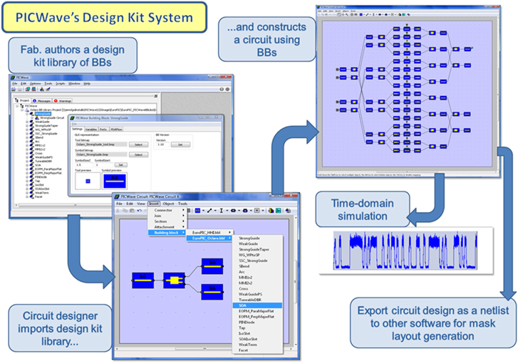
Figure 24. Design flow based on PICWave circuit simulator.
Download figure:
Standard image High-resolution image7.1.3. PICWave (Photon Design)
PICWave is a time-domain based photonic circuit simulator that is capable of modelling both passive and active components. Passive (linear components) can be specified by simple parameters like the optical length of a waveguide, or the coupling coefficient of a directional coupler; or alternatively a wavelength-dependent S-matrix. PICWave also has detailed models of active components such as SOAs, laser diodes and optical modulators. In contrast to passive components, where good surrogate models like the S-matrix formulation exist, it is difficult to create simple surrogate models, of an SOA for example, that match static and dynamic characteristics over a large operating range of temperature, electrical drive, optical input etc, at all modulation rates from MHz to 10's of GHz. Thus the PICWave active models include a lot of relevant physics such as carrier diffusion, spatial hole burning and current spreading.
Design kits using PICWave (figure 24) can provide the designer detailed models of their active building blocks that behave correctly over a wide range of operating conditions. This allows even the inexperienced circuit designer to include complex components like SOAs into a design without having to be an expert in optoelectronics modelling.
7.1.4. ADS (Agilent)
Agilent's Advanced Design System is an electronic design automation software tool for RF, microwave, and high speed digital applications. By adding custom modules it becomes possible to use ADS also for simulating complex Photonic ICs. COBRA has added many components ranging from single and multi-mode waveguides to MIRs and AWGs. The models employ an effective index based mode solver, and the simulation results are, therefore, firmly based on the physical properties of the circuit. With this approach, it is possible to see how the circuit responds to variations in etch depths or waveguide widths. Figure 25 shows a symbolic view of a PIC in ADS. The circuit consists of an AWG with one output channel connected to a FP cavity created by cascading two MIRs. The inset shows the simulation results, and the AWG channels plus the FP response can be clearly recognized.

Figure 25. Circuit schematic in ADS of an AWG connected to a Fabry-Perot cavity. Inset: wavelength response of the circuit.
Download figure:
Standard image High-resolution image7.1.5. Mask layout tools
After a circuit has been designed and optimized we want to validate conformity to the design rules of the foundry and generate the mask layout. Within the JePPIX consortium we are working with Mask Engineer from PhoeniX Software. Once a satisfactory design has been created with a specific foundry and package in mind, it can be transferred via the photonic design automation (PDA) framework to Mask Engineer.
With Mask Engineer the mask layout can be further completed and optimized (which is necessary because the circuit simulators cannot generate the full circuit mask layout) after which the PIC design is translated into mask files. During this process, automatic data processing takes place that obeys design rules set by the foundry. For example, a waveguide may have to be wider on the mask than in the original design in order to compensate for a known amount of under etch. Or the definition of a waveguide may involve a local mask inversion. In addition, the software will perform foundry specific design rule checks (DRC) at the logical and mask levels. The design can, for example, be checked for rule compliance on the minimum allowable bend radius, or a check may be performed to ensure that metallization and waveguide layers are neither overlapping nor closer than a minimum distance. All the building blocks are defined with stay out regions called bounding boxes to avoid overlaps and proximity effects in the InP process. Figure 26 gives an example of a mask layout element (a curved connector) and a mask layout view.

Figure 26. Example of a mask layout element and a mask layout view in Mask Engineer.
Download figure:
Standard image High-resolution imageWhen the PIC design is part of a Multi Project Wafer (MPW) run, a brokering organization (like JePPIX) will collect the mask files from all participating users and place them in individual reticle cells. When the mask set is ready, the wafers can then be processed by the foundry. If IP-protected or 'private' building blocks are used, the broker or the foundry will replace their bounding boxes with the actual mask layout. The foundry may also add process control features, alignment and cleaving marks, for example in the final stage of mask assembly.
7.1.6. PDAFlow API
In order to allow the efficient and error-free transfer of designs between different software packages, a standard interface, the PDAFlow API 20 , has been developed and is now available as an open standard for use by all photonics software vendors via www.pdaflow.org [91].
An API is a particular set of rules ('code') and specifications that software programs can follow to communicate with each other. It serves as an interface between different software programs and facilitates their interaction, similar to the way a (graphical) user interface facilitates interaction between humans and computers. The PDAFlow API has been developed to allow the different software tools as mentioned above to exchange data, to simplify the development of PKDs by foundries and to allow IP-block 21 (IPB) development by design houses and academic groups.
One particular advantage of working with the PDA-framework is that a foundry can make available unique building blocks that are covered by patents or trade secrets. The unique building block may contain IP owned by the foundry, one of the software tool developers or other designers and released for general use under license. These BBs are represented by a bounding box in the design kit that hides what is inside the box, but does detail the location of input and output waveguides, electrical connections as well as the functionality of the building block through a wavelength dependent scattering matrix or other models.
The API is an essential part of a horizontal development business model where independent companies provide different elements of a technical solution. Through standardization initiatives as the API the interfaces in a horizontal model between layers, be it software or technology, are well defined and accessible to developers and licensed users. It makes the system flexible to gradual upgrades and competition. IP-blocks in such a system can be used by developers and, very importantly, also licensed to outside users either individually or through support contracts, if desired.
7.2. Design manual
The Design Manual is a document that contains the information needed by a user to design an ASPIC on a platform. It can be provided directly by the foundry, but usually it is distributed through a brokering organization (JePPIX for the InP platforms). All relevant technical information about the building blocks that are available within the developed generic technologies at the foundries is consolidated into the Design Manual which describes the complete generic platform offering including information on the available chip sizes, packages and the use of the software tools.
7.3. PDK and component libraries
The PDK is a (licensed) plug-in library for the Software Environment containing the technology and/or foundry specific technology information such as set-up files for mask layer information, building blocks, design rules and design rule checking. The PDK may also contain layout information and templates for standardization of optical and electrical port positions. It is the responsibility of the foundry to ensure that it is correct and up to date.
An important part of the PKD is the Component Library. It contains the mask layout and a model description of a number of building blocks. The PDK may contain a number of component libraries owned by different parties, but provided by the broker or the foundry.
The Component Library contains as the most basic part a set of BBBs. The foundry may decide to make additional building blocks with higher complexity (CBBs) also available to the PDK users, on conditions to be determined by the foundry. In addition designers may also develop their own building blocks (CBBs; BBBs can be provided only by the foundry) and make them available to other designers via the PDK, or directly to the interested users. The conditions for using these can be chosen by the owner of the building block.
The component library enables the designer to use components (building blocks) without knowing all the details about their operation and fabrication. The potential of a foundry process is determined by its performance, but also by the number of building blocks that are available in the library. A foundry platform with a library containing a variety of well-defined building blocks for MMI-couplers, AWGs, amplitude, phase and frequency modulators, including complex modulators like DQPSK and PM-DQPSK modulators, SOAs, CW and pulse lasers with varying pulse widths and rates, tunable and multi-wavelength lasers, fast switches, wavelength selective switches, polarization converters, splitters, combiners and controllers, will cause a revolution in the way in which complex photonic ICs will be developed. Furthermore, once a building block is available designers can start to expand its application to even better performance, higher accuracies, more ports or more wavelengths, larger wavelength ranges, to mention just a few possibilities.
Creating accurate basic or CBB descriptions for the component library is a major effort. It requires a thorough analysis and optimization of the component and extensive characterization and testing in order to provide an accurate prediction of its performance. It will require an army of researchers for developing all those building blocks, but once we have a good library it will speed up the development of Photonic ICs by at least an order of magnitude and reduce the design cost accordingly.
The two main components of a building block description in the library are the mask layout and the model description.
The mask layout contains the layout information for all the mask layers that are used in the fabrication process. The designer can choose the position on the mask where to include the component, and the orientation of the component in the circuit. If the component is parameterized the designer can choose the value of a geometrical parameter (e.g. waveguide width, bending radius, section length of SOAs or phase modulators) or even an optical parameter for more advanced building blocks (like FSR for an AWG) within the design rules, which usually set limits on the range of possible values. The applied building block contains the detailed layout information, but as discussed earlier it may also show up as just a symbolic layout block which shows the position and the size of the component, including the location of the input and output ports for both the photonic and electric connections. For such protected or 'private' building blocks the detailed information is inserted by software owned by the foundry before the masks are fabricated. In this way, IP of the owner can be effectively protected. If the library provides a good model description of the building block the designer is not hindered by lack of knowledge of exactly what's inside the box.
So far mask layout can be generated either directly in the layout software or through the PDAFlow API from the circuit simulator. Optimization of the layout for minimal area usage and/or RF constraints is still required in the layout software. Longer term, auto-layout of a whole circuit starting from a symbolic circuit description may become feasible. But at the moment the interconnect problem (routing) has too many degrees of freedom and is too complex to be solved automatically. A number of semi-automatic interconnect tools are available to support the designer with this job.
The model description in its simplest form can be a written description of what a building block does, supported by some measured data on its performance. Research is on-going for developing software descriptions for the PDKs that can be used in connection with the circuit simulators. The most straightforward way to do this, at least for linear components, is by providing an S-matrix to the circuit simulator which describes the coupling between the different ports. In a more sophisticated form the S-matrix elements may be specified as a function of wavelength, polarization or waveguide mode. The model may contain a description of nonlinear behaviour of the materials inside the component, including effects of injected carriers. Doing this for all components described in sections 4 and 5, for all the platforms, is a huge effort which will take many years for many researchers, but it is key to the future application potential of the platform. Within the PARADIGM project a significant effort is directed towards creating building block descriptions for a number of passive devices and lasers. Since the benefit of this effort is shared by the end-users, a large cost reduction is achieved compared to traditional in-house development approaches.
8. Generic packaging
Integration is critical in reducing the number of packaged parts, and thus reducing sub-system cost, as evidenced by the acceptance of extensive integration in the emerging generation of 100 Gbit s−1 transceivers. In a generic foundry approach the costs of small and medium size chips are expected to drop below one hundred Euros already for small volumes. With such low chip costs the total costs of a module will be dominated by the package. Packaging technologies require, therefore, a comparable generic approach to ensure sustained cost reductions over time.
The normal procedure for photonics packaging (unlike microelectronics packaging) is to design a bespoke package to suit the chip with minimal attention to using a truly standard package. In a generic approach this process is reversed: a versatile standardized generic package is developed and the chip has to be designed such that it complies with the standard package. Such an approach requires standardization of the chip size and the optical and electrical interfaces. This means a paradigm shift in photonic packaging.
As it will not be possible to develop a single package that covers all possible ASPICs, the approach in generic packaging technology so far has been to develop a small set of packages that can be used for a large number of different ASPICs, e.g. a package that can handle up to ∼10 optical IO-ports, a large number of electrical dc ports (e.g. 40) and 10 rf ports, and one or two packages for smaller port counts. In the following we describe the on-going work in the PARADIGM project [40] to develop such a package.
8.1. A standardized package
The need for standardization of critical high volume high performance packaging has been recognized by the IEC, the International Electrotechnical Committee who have standardized the ROSA (receiver optical sub assembly) and TOSA (transmitter optical sub assembly) package formats used in many high speed transceiver products used in high volume for both datacom and telecom applications. These two packages are then combined to sit side by side in the transceiver. For the large ASPICs with enhanced functionality offered by PICs fabricated on a generic platform it is sensible to combine the footprint of the TOSA and ROSA to produce a single package capable of fitting within the standard transceiver package body.
The package is designed with the following features:
- Standardized package format (potential IEC adoption)
- Up to 12 optical input ports
- Up to 10 rf ports with 25 GHz bandwidth
- Up to 36 dc ports and high-current TEC connections
- Captures connectivity requirements for more than 80% of PIC designs so far in MPW runs.
- XFP and other electronics package compatible
- TEC support
- Flex PCB/lead frame/wire bond interface
- Pigtail and optical connector compatible
This new POSA (PIC Optical Sub Assembly) measures just 15.5 × 18 × 5 mm, with an internal active device cavity ∼10.5 mm square. The package, which has been shown in figure 27, has been designed in conjunction with one of the largest manufacturers of this style of package to ensure the highest performance, best price and manufacturability. This will ensure compatibility with many high volume ROSA and TOSA manufacturing lines and also with typical prototyping capabilities associated with many foundries. All of these factors should help minimize cycle times for new products with the best cost.
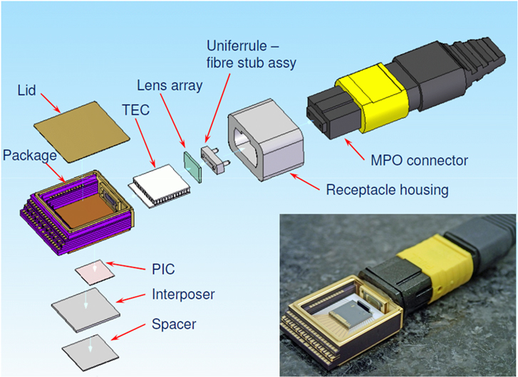
Figure 27. Exploded view of POSA package. Inset: test chip with lens array mounted in POSA package.
Download figure:
Standard image High-resolution image8.2. A standardized chip
To comply with a standardized package the optical and the electrical interfaces of the chip have to be standardized too, as well as its form factor. With the freedom that is offered to designers in positioning their components on the chip, it has turned out that fixing the positions of the optical input and output ports is not a large constraint, designers found it easy to comply with this standard. The requirement may introduce some additional waveguide length in the chip, but with a clever design this will be of order of a few mm maximum. Additional propagation losses in a low loss process are small.
Standardization of optical interfaces. For the optical ports the most important features of a standard for multi-port interfaces are the spot size of the optical ports and their pitch. For direct coupling to a fibre ribbon a spot size of ∼10 μm and a pitch of 250 μm are required. The Fraunhofer HHI (receiver-type) platform has a spot size converter (SSC) with such a large output spot. But for platforms that also include lasers and amplifiers enlarging the mode to such a diameter significantly complicates the process technology. The Oclaro (transmitter-type) platform has an SSC with a 3 μm, circular, output spot. This is considered a good compromise between integration process complexity and packaging complexity and it is adopted as a provisional standard within the JePPIX consortium. For the pitch an integer multiple of 25 μm is agreed. This is compatible with the 250 μm pitch of fibre ribbons, but it also allows much denser spacings which can be realized when coupling the chip to a high-contrast dielectric interposer chip. In order to support angled facets without having to rotate the optical chip special features are included in the chips in order to have a straight output beam also for angled facets.
Standardization of electrical interfaces is quite common in microelectronics. The most common approach for the dc-contact is to bring them to the edges of the chip and agree on size and pitch of the bond pads. This requires an interconnect plane that can cross the optical waveguide layer. The Fraunhofer HHI, COBRA and Oclaro platforms all offer this facility. For the rf-ports standardization is more complicated. For bringing the contacts to the edge of the chip an rf-interconnect plane with low rf losses would be required. This is not yet available in any of the JePPIX platforms.
Standardization of chip size. For the chip size a standard of 2, 4 or 6 mm for both dimensions of the chip has been agreed. This will reduce the number of different interposers that are required between the edge of the chip and the edge of the package.
The approach outlined in this section is still under development, but we are confident that it will not only bring us a strong reduction in packaging cost, but also in characterization cost and time, because the standard IO will also enable standardized test setups, which is the topic of the next section.
9. Generic testing
9.1. Wafer validation
In a generic process the performance of the process has to be validated for each wafer run; the customer will expect such a validation. Validating the process on the performance of user ASPICs is not practical in an MPW run; each ASPIC will require a different test setup and procedure, and failure of the ASPIC does not mean that the process failed, the problem can also be in the user design. The only practical way for validating a generic process is by including a test cell for the characterization of the BBBs. If the performance of the BBBs is OK, the performance of all components that are based on these BBBs should also be OK if they are properly designed and the process is sufficiently mature. By restricting the testing to the BBBs, we avoid ending up with a large number of building blocks, the testing of which will require impractically large test cells. Also for process technology development it is practical to have a small set of BBBs, on which the process optimization can be focused.
9.2. On-wafer testing
Testing optical components is more difficult than testing electrical components. First, optical ports are only accessible after the wafer has been diced, and second the alignment tolerances for accurate coupling of light in or out of a waveguide are tight, so testing is slow. Alignment tolerances for electrical measurements are larger because the electrical contacts are larger and the effect of some misalignment is small as long as the contact is good. A great advantage of electrical measurements is that they can be done on-wafer: it is not necessary to dice the wafer for testing, which makes automated testing much easier.
We are, therefore, investigating the possibility of on-wafer testing of the optical properties of the most important building blocks in Photonic ICs. In the PARADIGM project we are investigating two approaches: one is by integrating vertical output couplers in the chip that can be accessed by vertical optical probes. The other approach is by integrating the Device Under Test (DUT) between sources and detectors that are integrated in the chip. In this latter approach we make use of the relative ease with which test circuits, even complex ones, can be added into ASPIC designs, and of the excellent wafer uniformity. We will describe this approach briefly in this section.
A general approach for measuring transmission loss is by comparing it to the transmission of a reference device, usually a straight waveguide section. We can do this on-wafer by integrating the DUT and the reference device between an integrated source and an integrated detector, as depicted in figure 28, and measuring the transmission electrically by comparing the output currents of the detectors, under the assumption that the sources are identical. As a source we can use an integrated SOA section, which will generate a broad spectrum, so that the measured transmission will be averaged (weighted) over the full band. If we use an integrated DBR-laser as a source we can measure at a specific wavelength. The accuracy of the approach is dependent on the reproducibility of the integrated test sources and detectors.

Figure 28. Measuring optical transmission of a DUT by comparing it to transmission through a reference device.
Download figure:
Standard image High-resolution imageThe most important BBBs in the Oclaro and COBRA generic integration processes are passive waveguide devices, SOAs and phase modulators. Their most important properties are propagation loss, gain spectrum and electro-optic efficiency, respectively. To illustrate our approach we will discuss three structures that we are presently investigating to measure them with electrical probes.
Waveguide loss can be measured, in principle, by comparing transmission through a short and a long waveguide section. If the propagation losses are low, a long waveguide section will be needed to measure the losses sufficiently accurately, and the test structure will have a large footprint. Another approach is shown in figure 29. It is based on the fact that the transmission of ring resonators is very sensitive to the losses in the ring. For testing waveguide loss we insert a ring formed with an MMI-coupler between a tunable DBR laser with a monitor diode and a detector diode. By sweeping the wavelength and normalizing the detector current on the current of the monitor diode we record a curve as shown at the right of the figure. By measuring the extinction ratio between the maximum and minimum power we can determine the waveguide loss. For further increasing the measurement accuracy we can compare rings with the same curves but different lengths of the straight waveguide sections.
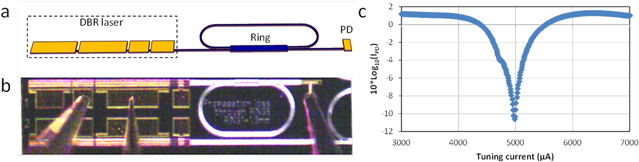
Figure 29. (a) Schematic, (b) microscope photo and (c) measured response of a test structure for on-chip measurement of optical waveguide loss.
Download figure:
Standard image High-resolution imageSOA gain. Figure 30 illustrates a test structure for measuring the gain spectrum of an optical amplifier. If SOA1 and SOA2 are identical the ratio of the output power from SOA1 with SOA2 on and off is the gain of SOA1. The gain measured in this way is the weighted average over the gain spectrum. If we insert an AWG behind SOA1 and have photodetectors connected to each output port, we can measure the spectral gain for each wavelength channel of the AWG. This will give us a sampled gain spectrum as depicted by the red dots in figure 30. A few channels will be sufficient for adequate validation of the SOA performance.
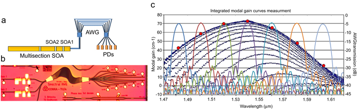
Figure 30. (a) Schematic, (b) microscope photo and (c) sampling principle of a test structure for on-chip measurement of spectral SOA gain.
Download figure:
Standard image High-resolution imageElectro-optic efficiency. A straightforward way to measure Vπ , the voltage at which a phase modulator introduces 180° phase shift, is to insert it into a MZI between an integrated source and detector, as depicted in figure 31, and record the transmission as a function of the voltage. Vπ is then the voltage difference between the two minima. In general it is voltage dependent, so a more sophisticated approach will be required to find the ϕ–V curve.

Figure 31. (a) Schematic, (b) microscope photo and (c) measured response of a test structure for on-chip measurement of the electro-optic efficiency of a phase modulator.
Download figure:
Standard image High-resolution imageThe three examples illustrate how optical or electro-optical properties can be measured on-wafer using electrical probes. In figure 5 the enlarged MPW cell appearing as an inset shows a test cell containing a number of test structures as described above. Such a test cell can be used for fast and accurate validation of the wafer, by measuring the performance of the BBBs and comparing it to the specifications.
10. Future prospects
Due to significant investments in developing a foundry technology infrastructure for InP-based monolithic integration and silicon photonics (well over 50 M€ in European and national projects) Europe is making substantial progress towards establishing this new way of working.
10.1. Technology development
Since 2007 COBRA has provided small scale access to a first generation (G1) InP-based research platform, as described in the present paper. Process capabilities are gradually being improved and presently support design of ASPICs integrating lasers, optical amplifiers, modulators and detectors with 10 Gb s−1 speed, and a variety of passive optical components. The platform is suitable for research and prototyping but not for volume production. In 2009 the EuroPIC project began with the mission of transferring the foundry model from a university environment to industrial and semi-industrial platforms (the wafer fabs of Oclaro and FhG-HHI) and starting development of software design kits and standardized packaging solutions. The capabilities of the EuroPIC platform technologies are listed in table 2, columns 2012. Some of the ASPICs developed in this project are described in section 6 of this paper. Results are very promising and the JePPIX platform [44] has started semi-commercial access to these foundry processes. Transition to full commercial operation is foreseen in 2015/16, provided the market demand justifies such a transition at that time.
In 2010 the PARADIGM project started with development of a second generation (G2) of platforms with improved capabilities and performance: capability of providing both transmitter and receiver functions with operation up to 40 Gb s−1, availability of superior lasers and amplifiers, wider choice of emission and detection wavelengths and other advanced features. The process will be competitive with advanced application specific technology, but at a much lower entry cost. Its targeted properties are listed in table 2, columns 2015. Further the project envisions development of low-cost generic packages and sophisticated PDKs with powerful component libraries, as described in sections 7 and 8. During the project small scale access is provided for selected external users. Assuming a viable business case, full commercial operation is envisaged around 2017, with earlier access for R&D purposes.
An important development is the integration of electronics and photonics in a single chip. In silicon photonics several groups have demonstrated integration of optical circuits in silicon membranes on silicon substrates, some of them also including active optical components like lasers. The main stream in integration of lasers in silicon photonics circuits is by bonding an InP-based III–V layer stack on top of the photonic silicon layer and processing the lasers in the III–V layer, and the other components in the silicon layer [92–94]. In this approach three layers will be required ultimately:
- (1)A CMOS electronic layer.
- (2)A silicon photonic layer.
- (3)An InP photonic layer.
Efficient coupling between the two photonic layers is difficult and requires significant real estate on the chip, especially if the active components get smaller. COBRA is following an approach in which the full photonic functionality is integrated in a single InP-based Membrane On Silicon (IMOS) thus reducing the number of layers to two by eliminating the silicon photonic layer and the coupling problems between the two photonic layers [95]. The technology could be implemented in a CMOS fab (with a dedicated process line) but also in an InP fab. It could become the third generation (G3) foundry technology merging InP photonics with silicon electronics.
10.2. Cost development
It is widely believed that InP PICs are much more expensive than silicon photonics PICs. By applying the generic foundry model the costs of InP PIC R&D and prototyping can be reduced by more than an order of magnitude which makes InP PICs very competitive with silicon photonics. Semi-commercial access to MPW runs is presently offered by JePPIX (www.jeppix.eu) for InP-based foundry processes and by ePIXfab (www.epixfab.eu) and OpSIS (www.opsisfoundry.org) for silicon photonics. For comparisons to be made the offered functionality and performance and the cost per square millimetre of design area are the most relevant figures. The number of chips delivered may also be relevant, but usually in the first stage only a few chips are needed for testing a new design. If we compare the most advanced Silicon Photonics processes with the most advanced InP based processes we see that in MPW runs InP offers significantly more functionality (lasers, optical amplifiers and better modulators) at lower cost, both for the price of participation in an MPW run as well as for the square millimetre price 22 .
For both technologies the cost for small scale production and prototyping will be dominated by the non-shared cost, whether this is the foundry process, the PDKs and IPBs, model development, characterization, software development or in the end the user-specific chip design time and resources. Here InP seems to have an advantage because R&D costs in large scale CMOS fabs are significantly higher than in smaller scale InP fabs, which makes the entry cost for generic InP technology lower than for silicon-photonics technology. For volume production the cost per square millimetre of InP foundry wafers is definitely higher than that of silicon photonics, essentially due to the smaller substrate wafers used and the smaller production volumes. At present they are in the range of 10–20 € mm−2, but this will decrease once the foundries get higher loads. Because of the higher R&D investments required for silicon photonics, InP may have a competitive advantage for small or even medium volume production.
For a fair comparison with silicon photonics we also have to include the packaging costs in the comparison. With the present photonic packaging technologies the costs of packaging are significantly higher than the chip costs, so for the final product the price of the chip is less important than the functionality that it integrates in the chip. As InP also integrates the lasers and optical amplifiers, which are required in most of the applications, the packaging costs will get lower than for silicon photonics chips where the lasers have to be integrated in a more costly hybrid way. So we expect that despite a higher square millimetre price packaged InP-PICs will be very competitive with packaged silicon photonics PICs.
10.3. Applications
The anticipated large reduction of R&D time and chip manufacturing costs will lead to a large growth of the share of PICs in the photonic components market. So far the commercial deployment of PICs has been mainly restricted to specific areas in telecom core-network applications, where their functionality cannot be matched by competing technologies. Telecom is a relatively niche area for the exploitation of photonic technologies, accounting for about 5% of the global photonics market [96]. Nonetheless the stringent requirements of telecoms are driving PIC research. Thus the opportunities to leverage PIC technology in other established photonic markets such as fibre sensor readout units, medical diagnostic, metrology and many applications where today's photonics does not provide a competitive price level, are immense. In section 6 a number of ASPICs for application in these markets have been discussed.
Another important advantage of the generic foundry approach is the short time-to-market. Because the ASPICs are developed in a qualified foundry process upscaling to larger production volumes is straight forward: once the ASPIC design meets the user requirements, the user can order a number of wafers in the same process in which he developed his ASPIC, which he can now fill completely with his design. For an ASPIC with 20 mm2 design area (4 × 5 mm2), a single 3'-wafer will contain more than 100 copies of the chip. So a volume of 100 000 chips is obtained with 1000 wafers, which can be easily handled by a medium-sized InP foundry.
Figure 32 shows the predicted development of the market enabled by InP-based ASPICS which was published in the JePPIX roadmap 2012 [97]. It was based on the expected growth of the number of ASPICs developed in MPW runs. In the figure the bars labelled 'Update 2013' indicate the actual numbers for 2012 and 2013, which are significantly higher than expected in 2011, when the graph was made. The sharp increase is partially due to the fact that the PARADIGM project offered access to a significantly higher number of users than originally expected, which will be lower in 2014. However, we expect that the availability of semi-commercial access in 2014 will compensate for this reduction.
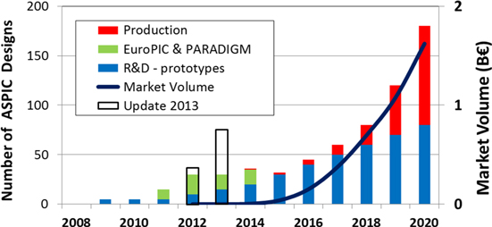
Figure 32. Development of the number of ASPIC designs in InP-based MPW runs (bars) and the market volume (line) as predicted in the JePPIX roadmap 2012 [97]. The figure has been updated with the actual figures of 2012 and 2013 (update 2013), showing a much faster development than anticipated in 2011.
Download figure:
Standard image High-resolution imageIn the JePPIX roadmap model the predicted market development is caused by a large number of small or medium volume applications with a high added value, rather than by a few low-cost 'killer' applications. This model provides an evolutionary path towards larger market volumes, which will enable the foundries to improve the performance and reduce the cost of the fabrication process in a number of smaller steps. Such cost reductions may eventually also enable low-cost applications in mass markets .
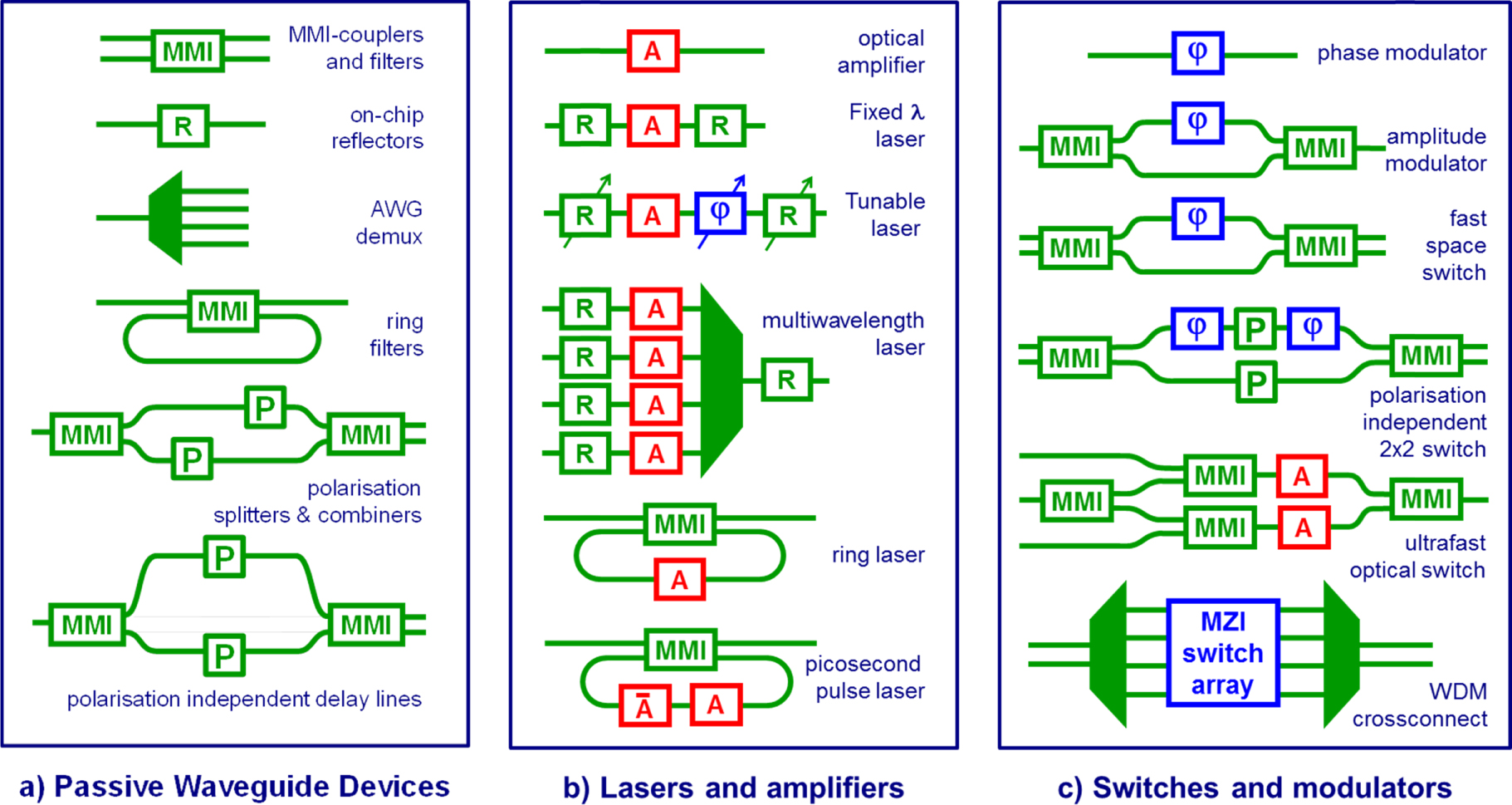
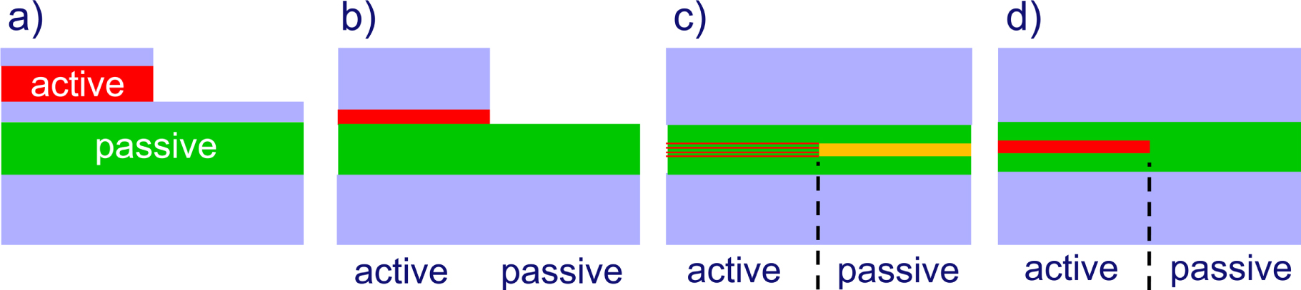
Figure 33. The relation between InP and silicon, left: on the shorter term, right: on the longer term.
Download figure:
Standard image High-resolution image
11. Conclusions
Generic InP-based foundry technology will lead to a dramatic reduction of the entry costs for companies that are interested in applying InP ASPICs in novel or improved products. It will bring advanced photonic InP-based integration technology within reach for many SMEs. Major R&D funding by the EU and national governments has brought the foundry approach to a level that experimental foundry runs have been demonstrated successfully on industrial integration platforms, and semi-commercial access to the foundry platforms has started in 2014. Significant progress has been made in the development of PKDs and standardization of packaging and at present InP PDKs support significantly more powerful component libraries than any other photonic integration technology that has open access.
Beyond prototyping runs through Multi Project Wafer services, we expect InP to be very competitive for small and medium volume production. Due to the nature of the production infrastructure the start-up costs are lower compared to advanced silicon photonics processes, while offering significantly more functionality. In the long term we expect InP-Photonics and CMOS electronics to merge in a heterogeneous integration technology, where CMOS will provide the electronic functionality and InP the photonic functionality.
Acknowledgements
Funding is acknowledged by the EU-projects ePIXnet [38], EuroPIC [39] and PARADIGM [40] and the Dutch projects NRC Photonics, MEMPHIS [41], IOP Photonic Devices [42] and STW GTIP [43]. Many others have contributed and the authors would like to thank other PARADIGM and EuroPIC partners for their help in discussions, particularly Michael Robertson (CIP).
Footnotes
- 17
Several metrics have been proposed for measuring chip complexity. We use a simple but coarse approach in which we count the number of basic components like AWGs, MMIs, SOAs, detectors and modulators. It does not count for the fact that a DFB laser is more complex than an MMI coupler, for example, so a higher number of components does not always mean a more complex chip. Further, we count only components that are essential for the PIC-functionality (e.g. no spare components that are not used).
- 18
A full list of the abbreviations used in this review is given in the appendix.
- 19
- 20
PDA = Photonic Design Automation, API = Application Programming Interface.
- 21
An IP block is any building block which has IP-protection. As the Basic Building Blocks are automatically licensed to the user by the foundry, IP protection is most relevant for Composite Building Blocks. So in practice an IP-Block is a CBB with IP-protection.
- 22
Price information for the silicon photonics platforms of IMEC and LETI can be found on the website of Europractice (www.europractice-ic.com/SiPhotonics_pricing.php) and for the IME platform on the OpSIS website (http://opsisfoundry.org/tapeout-schedule). Information about pricing of the InP platforms can be found on the JePPIX website (www.jeppix.eu/mpwruns/pricing).