
Abstract
The present paper focuses on the interactions between single SnS and SnS2 monolayers and the properties of the combined SnS@SnS2 double-layer system. These materials occur as structural elements in inorganic nanotubes. We have employed density-functional theory-based methods to calculate structural, energetic, and electronic properties of these structures. Thereby, we have put emphasis on the difference between the two single layers and the double-layer system with special consideration of an occurring charge transfer from SnS2 to SnS. We will show that the interlayer interplay is beyond a simple non-bonding van-der-Waals interaction, which contrasts the properties of many other layered structures and makes combined SnS@SnS2 a unique material.
Export citation and abstract BibTeX RIS
Introduction
Properties of two-dimensional (2D) inorganic materials became a focus in applied nanosciences as a result of emerging low-cost exfoliation techniques [1–3]. For applications, semiconducting layered transition metal materials [4] offer a reasonable alternative to graphene, which is disadvantageous due to the absence of a notable band gap. Wolfram and molybdenum disulfides and diselenides are direct band-gap semiconductors [5, 6] and predestined for applications in electronic devices [7–10].
Additionally, 2D layered nanomaterials can be viewed as basic source material or structural element for the generation of inorganic fullerenes, nanotubes, and other materials such as nanoscrolls or nanoonions. Although these nanostructures are not directly produced from layered material in the first place, their structure is governed by the properties of the original 2D layered materials. However, rare cases of nanotube generation through rolling up nanolayered materials are reported [11, 12]. A special case is, e.g., the generation of combined SnS@SnS2 nanotubes. In 2009, SnS2 nanotubes were synthesized for the first time from SnS2/SnS fullerene-like nanoparticles [13], which could be fabricated since 2003 [14].
These systems, SnS and SnS2, are in the focus of the present paper. Whereas MoS2 nanotubes have been investigated both experimentally and theoretically to a great extent [15–22], the situation is different for these compounds. SnS and SnS2 nanoparticles and nanotubes have been synthesized, not only as pure but also as mixed structures. Different types of stacking for SnS@SnS2 nanotubes were observed, and different structures, such as tubes and scrolls, were found [11]. These structures are estimated to form so-called misfit compounds, resulting from a lattice mismatch between the two original sublayers SnS and SnS2 [12]. Additionally, a stronger force than the van-der-Waals interaction between these two sublayers is assumed [11, 14].
To date, there have only been a few theoretical investigations of these systems [11, 23]. Even though, there are a lot of possible applications for these compounds: SnS and SnS2 are under investigation for possible optoelectronic devices, e.g. in thin film solar cells, SnS could be applied in solar absorbers [24]. Further applications might be near-infrared detectors and commercial semiconductors in the environmental industry and biomedical monitoring [25]. Because of its wider band gap, SnS2 can be used in solar cells [26] as well, and due to the empty sites in the structure of layered metal chalcogenides, these compounds are interesting as host lattices for intercalation reactions [27].
The two structures are shown in figure 1. SnS (figure 1(a)) has a layered structure with an orthorhombic unit cell and the space groups Pnma for the bulk phase and pmn21 for the single layer. Bulk α-SnS2 (figure 1(b)) crystallizes in the CdI2 structure with a hexagonal unit cell and the space group P m1. It has a layered structure as well with a trigonal unit cell, in which every single-layer consists of three atomic layers (sulfur–tin–sulfur). The sulfur atoms form a hexagonal close packing and the octahedral holes are filled with the tin atoms. As in graphite or other transition metal layered materials, e.g. MoS2, the individual layers are connected by weak van-der-Waals interactions, whereas the atoms of each layer are bonded by stronger covalent bonds.
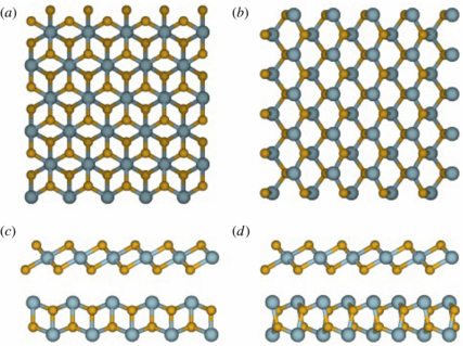
Figure 1. Top view of the (a) SnS2 and (b) SnS monolayers as well as side views of the combined SnS (lower layer) and SnS2 (upper layer) double layer for different orientations of these two layers relative to each other in (c) and (d). The tin and sulfur atoms are colored blue and yellow, respectively.
Download figure:
Standard image High-resolution imageIn the following, we will analyze and discuss results from quantum-chemical calculations of the structural, energetic, and electronic properties of layered SnS and SnS2 structures. We have calculated the energy levels, band gaps and densities of states for the isolated monolayers and bulk phases using density-functional based methods. Special emphasis has been put on the combination of an SnS and an SnS2 monolayer resulting in a super-structured double layer, for which we discuss an observed charge transfer between both layers. We will show that the interlayer interplay is beyond a simple non-bonding van-der-Waals interaction, which contrasts with many other layered materials and nanotubes and makes combined SnS@SnS2 layers a unique material.
Computational details
For the present study, we have utilized a density-functional tight-binding (DFTB) [28–30] method for the structural optimization of the investigated layered materials and for the calculation of their electronic structures as well as the band gaps and energies. It is based on the density-functional theory of Hohenberg and Kohn [31] in the formulation of Kohn and Sham [32]. The Kohn–Sham orbitals ψi( ) are expanded in a set of atom-centered basis functions φj(
 ). These functions are determined by self-consistent density-functional calculations on the isolated atoms employing a large set of Slater-type basis functions.
The effective one-electron potential in the Kohn–Sham Hamiltonian is approximated as a superposition of the potentials of neutral atoms. Moreover, only one- and two-center integrals are calculated to set up the Hamilton matrix. We have taken a minimal valence basis including the 3s, 3p, and 3d orbitals for sulfur and the 5s, 5p, and 5d orbitals for tin. States below these levels were treated within a frozen-core approximation. All calculations have been performed using the program packages deMonNano [33] and DFTB+ [34] with rectangular periodic boundary conditions.
For comparison, the electronic structures and the energies of the crystal orbitals have been calculated also with full density-functional theory (DFT) using a Perdew–Burke–Ernzerhof (PBE) exchange-correlation functional [35] with a double-zeta plus polarization (DZP) basis as implemented in the Siesta [36] program package; rectangular periodic boundary conditions have been applied as well.
The band gaps of the bulk phases and single layers have been obtained from the band structures which have been calculated for the primitive cells along all symmetry lines. The total and partial densities of states have been calculated for rectangular supercells with an edge-length of approximately 20 Å containing 100 SnS and 108 SnS2 atoms, respectively. For these calculations a set of 25 optimized k-points (Monkhorst–Pack) have been used.
Results
The band structures and the energies of the crystal orbitals for the bulk structure and the monolayers of both materials have been calculated using the DFTB approach and full DFT. From these calculations, the band gaps, which turned out to be indirect in all systems, have been received and can be compared to available experimental values (table 1). Full DFT calculations underestimate the band gap of the bulk phases. As we can see from table 1, the band gaps calculated here by the DFTB method are closer to the experimental data. Additionally, the data shows that the calculated monolayer band gaps are always larger than those of the corresponding bulk structures.
Table 1. Band gaps calculated by DFTB and full DFT for SnS and SnS2 monolayers and the bulk phases. The experimental values refer to the bulk phases and are given for comparison.
| DFTB (eV) | DFT (eV) | Experiment (eV) | |
|---|---|---|---|
| SnS monolayer | 2.61 | 1.68 | |
| SnS bulk | 0.89 | 0.87 | 1.1 [37] |
| SnS2 monolayer | 2.81 | 1.61 | |
| SnS2 bulk | 2.55 | 1.36 | 2.3 [38] |
Figure 2 shows the total density of states (DOS) for the SnS and SnS2 monolayers, and an overview of the main contributions to the electronic bands is given in table 2. The occupied bands in the range of −16 to −19 eV consist of sulfur s states in both systems. In the SnS layer, the additional occupied bands below the Fermi level are composed mostly of sulfur p and tin s (−5 to −7 eV, −10 to −12 eV) and p contributions (−5 to −10 eV). The unoccupied bands result mainly from sulfur d and tin p and d states.

Figure 2. Total DOS (calculated by the DFTB method) of the SnS (top, black) and SnS2 (bottom, blue) monolayers with respect to the vacuum zero. The respective Fermi energies εF are marked by vertical dashed lines.
Download figure:
Standard image High-resolution imageTable 2. Main contributions to the electronic bands in the DOS of the SnS and SnS2 monolayers in the energetic range that is shown in figure 2.
| SnS | SnS2 | ||
|---|---|---|---|
| Energetic range (eV) | Major contribution | Energetic range (eV) | Major contribution |
| −16 to −19 | Sulfur s states | −16 to −19 | Sulfur s states |
| −10 to −12 | Sulfur p and tin s states | −6 to −12.5 | Sulfur p and tin s states |
| −5 to −10 | Sulfur p and tin p states | −7.5 to −10 | Sulfur p and tin p states |
| −5 to −7 | Sulfur p and tin s states | −6 to −7.5 | Sulfur p and tin d states |
| −2 to 5 (unocc.) | Sulfur d, tin p and d | −3.5 to −1 (unocc.) | Sulfur p and tin s states |
| states | > −1 (unocc.) | Sulfur d and tin p and d | |
| states | |||
A similar behavior can be observed in the SnS2 DOS: the occupied bands in the range of −6 to −12.5 eV are composed of mostly sulfur p and tin s (−10 to −12.5 eV), p (−7.5 to −10 eV) and d states (−6 to −7.5 eV). The unoccupied bands from −3.5 to −1 eV are primarily tin s and sulfur p states, whereas the states beyond −1 eV are sulfur d and tin p and d states. In total, the occupied bands of the two densities of states are quite similar; the main differences occur close to the Fermi levels. Thus, we see that the d orbitals, which are unoccupied in the free atoms, strongly influence the electronic structure of these layers.
The DOS of the combined SnS@SnS2 double layer is shown in figure 3. We have added as well the sum of the densities of states of the isolated SnS and SnS2 monolayers (as shown in figure 2). Both curves have a similar progression. However, the important difference becomes apparent at the occupied states close to the Fermi level: here, additional states appear in the DOS of the interacting double layer in contrast to the simple sum of the DOSs of the single layers indicating electronic interactions between the layers. These bands mainly consist of sulfur p and tin s and p states of the SnS layer, whereas the first unoccupied bands beyond the Fermi energy mostly consist of sulfur p and d states of the SnS2 layer. Consequently, the band gap in the combined system decreases to approximately 1 eV, and electron density is transferred from the SnS2 to the SnS layer resulting in additional occupied SnS states close to the Fermi level.

Figure 3. DOS of an SnS@SnS2 double layer as shown in figure 1 (c), calculated by the DFTB method. The black curve represents the DOS of the combined layers, whereas the red curve illustrates the summation of the DOSs of the two isolated monolayers (cf figure 2). The blue dashed curve shows the difference between these two curves (right axis of ordinate).
Download figure:
Standard image High-resolution imageThe interaction energy between a single SnS and a single SnS2 layer as function of the interlayer distance d is depicted in figure 4. The two layers are stacked as shown in the inset, in which d is the distance between the opposing atoms in both layers projected in z direction (perpendicular to the layers). The two curves result from DFTB calculations with and without specific London dispersion correction [39]. Both curves have an energy minimum at a distance of approximately 3.2 Å resulting in a total thickness of the combined double layer SnS@SnS2 of 12 Å. This fits very well to the experimentally received double-layer thickness in SnS@SnS2 nanotubes and nanoscrolls, which is measured as 11.5 Å [11]. Although the interaction energy of the system modeled without London dispersion correction is approximately 0.12 au (∼0.013 eV/atom), this energy gain already indicates an interlayer interaction beyond pure van-der-Waals forces.
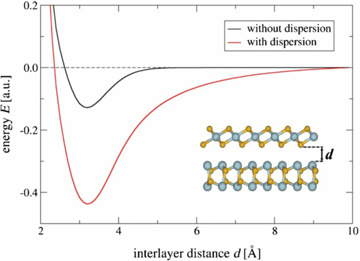
Figure 4. Total energy as function of interlayer distance of a combined SnS@SnS2 double-layer system with (red) and without (black) a London dispersion correction incorporated in the DFTB description. The inset shows the two layers and the definition of the interlayer distance as the projection of the difference in z component of the opposing inner atoms.
Download figure:
Standard image High-resolution imageTo get a visual picture of the transferred charge, we employed the concept of Mulliken populations and calculated the Mulliken charge variations that occur when combining the two monolayers to a double layer. The result is shown in figure 5. This figure depicts the individual atomic charge as a function of its z component (z is the axis perpendicular to the layers). Whereas the charges of the SnS2 atoms either stay constant or decrease, all atoms in the SnS layer gain electron density. This is a clear indication for a charge transfer from SnS2 to SnS, although the transfer is quantitatively very small (approximately 0.1 electron per SnS2 unit). Additionally, we see a broad variation of charges close to the interface, which is due to the incommensurability of the two structures. The spreading declines with increasing distance to the interface, and the charges approach the charges of the isolated systems.

Figure 5. Atom-resolved changes in the Mulliken charges of an SnS@SnS2 double layer with respect to the isolated single layers (cf figure 1). If the Mulliken charge of an atom in the combined system is the same as in the single layered system, Δq = 0. The ordinate refers to the position in the layers. (The crosses represent the charges of the individual atoms in both layers.)
Download figure:
Standard image High-resolution image
The simple picture that results from using the energy levels of the single monolayers is clearly not enough for a correct description of the electronic structure of the double-layer system. This holds for the energy levels themselves as well as for the summed DOSs, and it is independent of the theoretical method. The results from the combined system give strong hints on the existence of charge transfer from the SnS2 to the SnS layer: with occupied states close to the Fermi level, a smaller band gap, Mulliken charge variations, and an interaction energy beyond pure van-der-Waals forces arising. These results will be used for further investigations of large nanotubular SnS@SnS2 structures.
Conclusions
In this paper, we have presented a computational and theoretical investigation of structural, energetic, and electronic properties of SnS and SnS2 monolayers and the combined double layer. We have employed a density-functional tight-binding method, which gave access to large systems with several hundred atoms. Additionally, full DFT calculations for the band structures of the monolayers and bulk phases have been performed for comparison.
We observed the band gaps to be larger in the monolayers than in the bulk structures. This is independent of the system and the method. Furthermore, good accordance of the values calculated with the DFTB method with the experimental gaps in the bulk systems has been received.
The formation of an SnS@SnS2 double layer from an SnS and an SnS2 monolayer leads to the same energetically preferred structure independent of the consideration of dispersion interactions between the single layers. In the DOS of the double layer, additional states resulting from sulfur p and tin s and p states of the SnS layer arise near the Fermi level compared to the summed DOSs of the two isolated monolayers. The Mulliken charges clearly indicate a charge transfer from the SnS2 to the SnS layer. Although this effect is quite small, it leads to an additional interaction between the layers resulting in a larger stability of the double layer. This might be one reason, why experimental observations of nanosystems, e.g. nanotubes or nanoscrolls [11, 12], often reveal the simultaneous presence of SnS and SnS2 layers.
Acknowledgments
This work was financially supported by the European Union via ERC grant INTIF 226639. Furthermore, we thank Reshef Tenne, Gal Radovsky, and Igor Baburin for fruitful discussions.