
Abstract
This paper presents an in-depth review of the memristor from a rigorous circuit-theoretic perspective, independent of the material the device is made of. From an experimental perspective, a memristor is best defined as any two-terminal device that exhibits a pinched hysteresis loop in the voltage–current plane when driven by any periodic voltage or current signal that elicits a periodic response of the same frequency. This definition greatly broadens the scope of memristive devices to encompass even non-semiconductor devices, both organic and inorganic, from many unrelated disciplines, including biology, botany, brain science, etc. For pedagogical reasons, the broad terrain of memristors is partitioned into three classes of increasing generality, dubbed Ideal Memristors, Generic Memristors, and Extended Memristors. Each class is distinguished from the others via unique fingerprints and signatures. This paper clarifies many confusing issues, such as non-volatility, dc V–I curves, high-frequency v–i curves, local activity, as well as nonlinear dynamical and bifurcation phenomena that are the hallmarks of memristive devices. Above all, this paper addresses several fundamental issues and questions that many memristor researchers do not comprehend but are afraid to ask.
Export citation and abstract BibTeX RIS
1. If it's pinched it's a memristor
In this paper, any two-terminal black box is called a memristor [1] if, and only if, it exhibits a pinched hysteresis loop 1 for all bipolar periodic input current signals (resp., input voltage signals) which result in a periodic voltage (resp., current) response of the same frequency, in the voltage–current (v–i) plane. The concept of a memristor was first introduced in [3] as a two-terminal circuit element that links the remaining missing pair of four basic circuit variables, namely, flux and charge. It was formally defined as the fourth circuit element [4] and christened memristor (portmanteau for memory resistor) in 1971 [1].
Our above definition of the memristor in terms of a 'pinched hysteresis loop' in the v–i plane is consistent with the original definition of the ideal memristor in [1], but also encompasses the generalized definition in [46], for memristive devices. Pinched hysteresis loops are in fact the hallmarks of all memristors, ideal or otherwise. Since it is based entirely on experimental measurements, with periodic testing voltage or current signals, it is an 'operational' definition that does not require an a priori mathematical model. In other words, whereas the definitions in [1, 2, 4] and [46] are formal mathematical models of memristors with different degrees of generality, the pinched hysteresis loop captures the essence exhibited by all of these mathematical models, including the ideal memristor and generalized memristor adopted in [4] to cover the original terminology in [1] and [46] respectively, as well as the additional new terminologies dubbed extended memristor, generic memristor, and ideal generic memristor defined in section 2. These new terminologies are introduced for pedagogical reasons and should not be interpreted as new types of memristors. They represent merely finer memristor subclasses that possessed distinct mathematical formulas. Such finer classifications are useful because each subclass is endowed with unique features that allow researchers to identify by merely applying different testing signals.
In the following subsections, we will present numerous examples of real two-terminal electrical devices that we have identified from several unrelated disciplines which exhibit a 'pinched hysteresis loop' response to any bipolar periodic input voltage (resp., current) signal waveform with zero mean, i.e., with zero dc component.
1.1. First man-made memristor
In his quest to develop an electrical lighting device that would replace the prevailing gas lamps, Sir Humphry Davy [5] built a two-terminal electrical device consisting of two oppositely-directed sharply-honed carbon rods, separated by a narrow air gap, as shown in figure 1(a) [6]. When Davy applied a very high dc voltage (more than 1000 V, generated by connecting more than a thousand Volta batteries in series) across his carbon-rod device in 1801 [5], barely a year after Alessandro Volta invented the battery, a very bright continuous electric arc discharges across the air gap, thereby heralding the world's first electric lamp2 . Until only very recently, Davy's arc lamp had been misidentified as a light-emitting resistor. We now know it is in fact a memristor (Lin, et al [7]), as confirmed in a recent elaborate laboratory experiment at the University of Hong Kong, where a low-voltage scaled version of Davy's carbon rod arc discharge device was built (figure 1(b)), and the associated voltage and current waveforms were recorded (figure 1(d)). Observe the two waveforms are 'in-phase' in the sense that the current response i(t) = 0 whenever the input voltage v(t) = 0, which is the 'signature' of a memristor. The Lissajoux figure of the two waveforms (v(t), i(t)) in the i versus v plane in figure 1(e) shows the distinctive 'pinched hysteresis loop' fingerprint of a memristor3 .

Figure 1. Sir Humphry Davy's arc lamp is a memristor. (a) Davy's sketch of his carbon arc device. (b) Modern voltage-scaled version of Davy's Carbon arc device. (c) Davy's demonstration of his arc lamp to members of the Royal Institution in London in 1813. The lower part shows the picture of the huge bank of Volta batteries. (d) Voltage and current waveforms measured from the carbon arc device. (e) Pinched hysteresis loop associated with  from (d).
Download figure:
Standard image High-resolution image1.2. Pre-1948 memristors
Sir Humphry Davy's arc lamp was the first written record of artificial lighting without using fire [5, 6]. His invention led quickly to the commercialization of various types of discharge tubes, as chronicled in a 1948 gem by Francis [8]. We have extracted the v–i Lissajoux figures of four discharge tubes from [8] and redrawn them in figure 2. Though unbeknownst to the makers of these discharge tubes, their measured Lissajoux figures bore the fingerprints of memristors.

Figure 2. Pinched hysteresis loops of four discharge tubes made before 1948. Extracted from V I Francis' 1948 book (Fundamentals of Discharge Tube Circuits) [8].
Download figure:
Standard image High-resolution imageA careful analysis of discharge tubes in [7] and [8] had confirmed that the Lissajoux figures of the devices measured from any zero-mean periodic input voltages or currents are pinched hysteresis loops. It follows from our experimental definition that discharge tubes are memristors.
1.3. Pre-1970 thin oxide-film memristors
The earliest memristors using thin oxide films between 150 and 1000 Å thick were reported by Hickmott [9] in 1962, and by Argall [10] in 1968. Two pinched hysteresis loops from Hickmott [9] were redrawn with the missing components in the third quadrant (assuming the Lissajoux figure is odd-symmetric) and shown in figures 3(a) and (b). A pinched hysteresis loop from Argall [10] is redrawn and shown in figure 3(c). They all bore the 'Pinched hysteresis loop' hallmarks of memristors.

Figure 3. The i versus v Lissajoux figures of 3 pre-1970 thin oxide-film devices are all pinched hysteresis loops.
Download figure:
Standard image High-resolution image1.4. 1971: synthesized memristors
As a proof of principle, a working memristor was synthesized, via a nonlinear circuit theory method developed in [3], and built using operational amplifiers (op amps) and transistors, as shown in figure 4. For a circuit engineer who needed a memristor device with the q versus φ curve shown on the bottom left of figure 4, for some novel applications, the black box in figure 4 would work just like a physical memristor, provided the operating frequency and dynamic range of all voltages and currents inside the black box are within the linear operating range of the op amps and transistors. Indeed, it was shown in [1] and [3] that a memristor with any prescribed q versus φ curve can be built using a resistor-to-memristor mutator as depicted in figure 5, and a nonlinear resistor having the same characteristic curve albeit replotted in the current i versus voltage v plane, which is a relatively easy task to build [3]. There are many ways to build a resistor-to-memristor mutator, the circuit inside the black box in figure 4 is only one possible realization. There are also many methods to build the 'surrogate' nonlinear resistor [3].

Figure 4. The charge q versus φ relationship measured across the two external terminals connected to the 'synthesized active circuit' inside the black box is virtually identical to the current i versus v relationship of the nonlinear resistor (also synthesized with off-the-shelf components).
Download figure:
Standard image High-resolution image
Figure 5. The 2-port defined in (a) is called a Resistor-to-Memristor mutator [3]. The theorem highlighted in (b) provides a systematic method to build a memristor whose prescribed q versus φ curve can be emulated by a two-terminal nonlinear resistor which in turn can be built with off-the-shelf solid state devices, such as pn junction diodes, zener diodes, etc [3].
Download figure:
Standard image High-resolution imageIt follows from the above scheme that memristors characterized by any prescribed q versus φ curve can be built with active circuit components, and a power supply, even if the desired memristor is passive, and therefore should not need an internal source of power. This power supply requirement is the main reason why the memristor had been relegated as an abstract device with no practical significance, until hp rekindled the interest with its titanium dioxide hp memristor in 2008 [11], a two-terminal passive nano device that measures less than 50 nm in diameter, and endowed with a non-volatile memory.
The seminal 2008 Nature paper has triggered unprecedented worldwide interests from both industry and academia, with publications increasing at an exponential rate. Most recently an 8 nm × 8 nm memristor was reported in [56], and a 1 nm memristor can be expected in the near future. For a state-of-the-art review, the reader is referred to three recent Special Issues on memristors, namely, Applied Physics A: Material Science and Processing (vol. 102, 2011), Proceedings of the IEEE (vol. 100, 2012), and Nanotechnology (vol. 24, 2013).
From the historical perspective, we end this section with the following quotation from the last paragraph (page 519) of [1]:
Indeed, in the same year (1971), M Kikuchi et al had published a paper in the journal Solid State Communications [12] where we reproduced the top of the paper below.
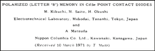
Kikuchi et al must have been flabbergasted by the strange current versus voltage hysteresis loop shown in figure 2 of their paper, which differs distinctly from conventional hysteresis loops from magnetic cores. Obviously sensing the importance of this new peculiar 'pinched' v–i loop, they added the adjectival name (LETTER '8') to the title of their paper. The following year, a review paper by H K Henisch on 'Amorphous Semiconductor Switching' confirms the generic feature of 'pinched' hysteresis loops for a class of memory devices dubbed 'ovonic memory switches', as depicted in figure 6(b) [13].

Figure 6. Two pinched hysteresis loops published around the same time as the memristor paper [1]. (a) A Letter-8 pinched hysteresis loop [12]. (b) A variant of a Letter-8 pinched loop exhibited by an 'ovonic memory switch'.
Download figure:
Standard image High-resolution image1.5. Post-2000 memristors
This subsection exhibits a cornucopia of pinched hysteresis loops measured from real memristor devices, kicked off by the influential paper by Beck et al [14] published at the dawn of the new millennium. They are ordered not chronologically, but in accordance with certain similar features that can be emulated by simple mathematical equations and circuit models. Figure 7 presents 6 typical pinched hysteresis loops sampled from the following papers and redrawn in color:
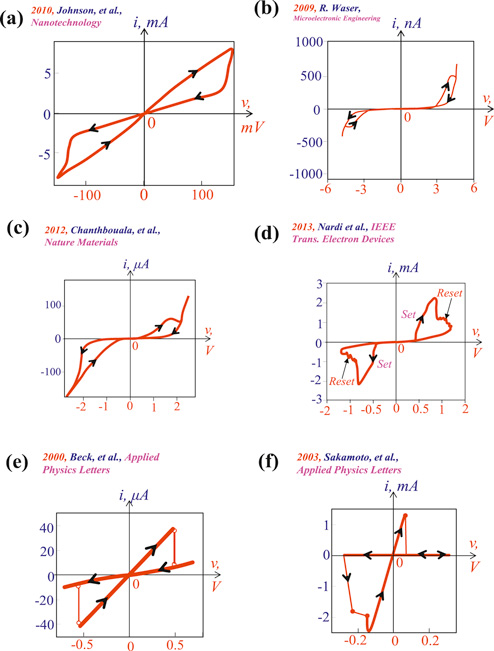
Figure 7. Six samples of pinched hysteresis loops measured from solid state memristors.
Download figure:
Standard image High-resolution imageFigure 8 presents six generic features of pinched hysteresis loops sampled from the following papers and redrawn in color:

Figure 8. Six more samples of pinched hysteresis loops measured from solid state memristors.
Download figure:
Standard image High-resolution imageThe family of pinched hysteresis loops exhibited in figures 7 and 8 are merely samples from publications that exhibit certain common morphologies. Unlike some devices such as those reported in [53] where a realistic physical model exists but did not include a pinched hysteresis loop in the v–i plane in linear scale, these samples are chosen for pedagogical reasons and do not imply superior performance over other uncited devices.
1.6. Organic memristors
The memristors listed in figures 7 and 8 are made from inorganic semiconductors or amorphous materials. Figure 9 shows an example of a pinched hysteresis loop measured from a memristor made from an organic material [26]. Unlike the preceding pinched hysteresis loops, note that the 'pinched' point is not at the origin, but nearby. Such offsets are usually observed from memristors made from organic materials and/or biomaterials. This departure from the original definition of memristors can be modelled by adding parasitic circuit elements and/or batteries [27]. We will henceforth refer to such memristors with a pinched point located near but not on the origin (v, i) = (0, 0) as an imperfect memristor.

Figure 9. Pinched hysteresis loop measured from an imperfect memristor whose pinched point is located near but not on the origin (v, i) = (0, 0).
Download figure:
Standard image High-resolution image1.7. Biological memristors
Many biological systems exhibit memristive behaviors. Figure 10 shows the current response when a sinusoidal voltage is applied to the ventral forearm as depicted in figure 10(a). The conductivity of the skin is often found to increase with the passage of current. This well-known phenomenon has been reported in [28] and can be explained by the electro-osmotic transport of fluid through pores in the skin, mostly through the sweat ducts. The physical mechanism responsible for the conductivity modulation in sweat pores has been reported in [29]. Applying a current across a sweat duct turns the skin into a memristor. In particular, conductive fluid flowing up the sweat pore helps the current to flow across it as illustrated in figure 10(b). Conversely, conductive fluid flowing down the sweat pore would increase the skin resistance. A typical pinched hysteresis loop in the v versus i plane measured from the set-up in figure 10(a) is shown in figure 10(c). Figure 10(d) shows a non-periodic current response during a transient regime upon application of a sinusoidal voltage. Observe that even though the current is not periodic, the current waveform (blue) i(t) passes through zero at the same times as the periodic sinusoidal voltage waveform (red) v(t), which is the signature of a memristor. Indeed, such phenomenon implies that our body is covered with memristors [29].

Figure 10. Experiments for demonstrating the sweat ducts in the skin are memristors.
Download figure:
Standard image High-resolution imageAnother biological system which behaves like memristors is the Amoeba (slime mould). A recent experiment reported in [30] clearly shows a pinched hysteresis loop when a slow periodic voltage is applied to an amoeba via a pair of silver wire electrodes as shown in figure 11. Note that the pinched point is located not at, but near, the origin (v, i) = (0, 0).
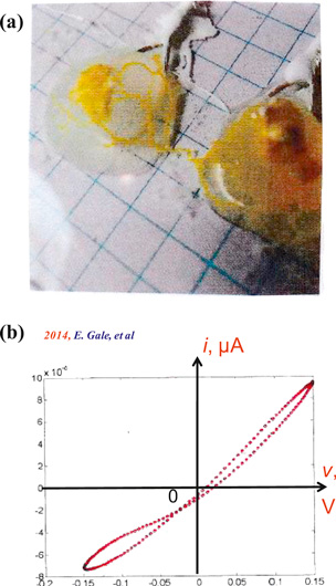
Figure 11. Experiments showing the Amoeba behaves like memristors. (a) The two narrow white objects on top of the yellow color amoeba are the silver wire electrodes where a voltage signal is applied. (b) A pinched hysteresis loop recorded from the experiment reveals a small offset of the pinched point from the origin.
Download figure:
Standard image High-resolution image1.8. Plant memristor
Many plants also exhibit memristive behaviors. Figure 12 shows the pinched hysteresis loop measured by applying a very slow sinusoidal voltage to a leaf of the venus flytrap plant [31], via a pair of Ag/Agcl+ electrodes. Observe the pinched point of the hysteresis loop is located not at, but near, the origin.
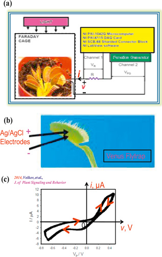
Figure 12. The pinched hysteresis loop in (c) is measured with the experimental set-up in (a), with a pair of Ag/AgCl+ electrodes attached to a leaf of the Venus Fly trap in (b).
Download figure:
Standard image High-resolution imageA similar experiment on the Mimosa Pudica plant also shows a pinched hysteresis loop in figure 13 [31].
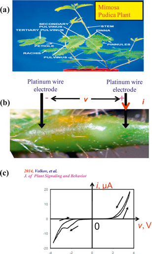
Figure 13. Applying a sinusoidal voltage across a pair of platinum wire electrodes attached to the pulvinus (lower right junction in (a)) of a mimosa pudica plant in (b) gives the pinched hysteresis loop in (c).
Download figure:
Standard image High-resolution image1.9. A micro kinetic memristor
Figure 14(a) shows a pair of bimorph coils attached between a pair of electrodes (memristor terminals) spaced about 200 μm apart. The dual coil was fabricated with a 30 nm thick layer (yellow) of cromium sitting on top of a 150 nm thick layer of vanadium dioxide (green) [32]. Application of a 3.1 V dc voltage across the two memristor terminals induces a rapid and powerful mechanical recoil resulting from a sudden decrease in the curvature of the coils and a corresponding increase in the coil diameter due to Joule heating. As shown in figure 14(b), the coil diameter increases with a corresponding decrease in the number of spiral turns because the length of the stretched wire remains unchanged. A tiny object placed in the center 'basket' notch will be hurled away like a catapult [32] with a force 1000 times more powerful than a human muscle of comparable size. In particular, this two-terminal device can catapult objects 50 times heavier than itself over a distance five times its length, and at a speed faster than the blink of an eye. A measurement of its current versus voltage characteristic shows a pinched hysteresis loop whose lobe area shrinks as the excitation frequency of the applied sinusoidal voltage increases, as depicted in figure 14(c). All of these observations bore the fingerprints of a memristor. Observe that the pinched point of the hysteresis loop in figure 14(c) of this micro catapult memristor is located at the origin (v, i) = (0, 0).
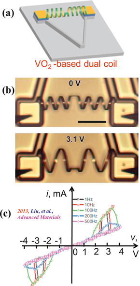
Figure 14. A micro catapult memristor. (a) A dual coil between two terminal electrodes. (b) The coil diameter increases with a corresponding decrease in coil curvature upon the application of a 3.1 V dc voltage. (c) The pinched hysteresis loops shrink in size as the frequency of the sinusoidal voltage excitations increases from 1 Hz to 500 Hz.
Download figure:
Standard image High-resolution image2. Three memristor representations
There are three mathematical representations of time-invariant memristors, each one has two forms depending on whether the input signal is a current source (current-controlled memristor) or a voltage source (voltage-controlled memristor). In the following subsections, we will present these three representations, in the order of decreasing generality.
2.1. Extended Memristor
An Extended Memristor is defined in table 1 (page 11).
Table 1. Extended Memristor
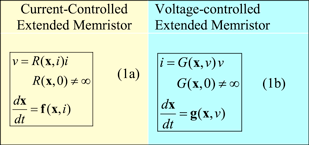 |
2.2. Generic memristor
A Generic Memristor is defined in table 2 (page 12).
Table 2. Generic Memristor
 |
2.3. Ideal memristor
An Ideal Memristor is defined as in table 3 (page 12).
Table 3. Ideal Memristor
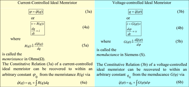 |
2.3.1. Memristor siblings
Every ideal memristor can be recast into a Generic Memristor with a scalar state variable x defined via a differentiable one-to-one function, in three simple steps as presented in table 4 (page 14).
Table 4. How to Create Ideal Generic Memristors
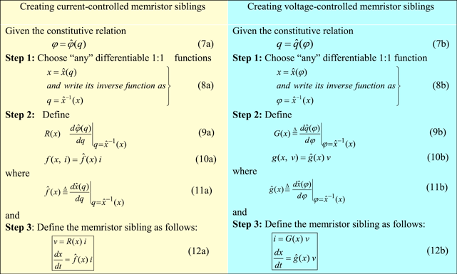 |
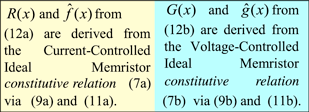
Since the function  in (8a) (resp.,
  in (8b)) can be chosen to be any differentiable one-to-one function, it follows that every Ideal Memristor has an uncountable number of memristor siblings that would give the same voltage response to a given input current i(t) (resp., the same current response to a given input voltage v(t)). Indeed, every Ideal Memristor is the mother of an infinite family of equivalent Generic Memristors.
2.3.2. Ideal generic memristor
We will henceforth refer to a small subclass of Generic Memristors as Ideal Generic Memristors if, and only if
Given a Generic Memristor described by (12a), or (12b), how does one determine whether it can be given the accolate of an 'Ideal' Generic Memristor ? The answer is to recast the second equation in (12a) and (12b) into the form:
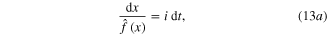

Integrating both sides of (13a ) and (13b ), we obtain


It follows from (14a ) and (14b ) that this Generic Memristor is an Ideal Generic Memristor if, and only if, F(x) (resp. G(x)) is a one-to-one function, in which case, we can rewrite (14a ) (resp., (14b )) via its inverse function; namely4 ,


where  (resp.,
  ) is the differentiable one-to-one function from (8a) (resp., (8b)).
We will end this section with an example for illustrating the above simple procedure for creating generic memristor siblings from an ideal memristor.
Example: Creating an Ideal Generic Memristor Sibling
Step 1. Choose any constitutive relation of an ideal memristor:
For this example, let us choose

Step 2. Choose an arbitrary differentiable one-to-one function:
For this example, let us choose

and its inverse

Step 3. Applying (9a) to (16)
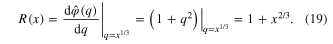
Step
4. Applying (11a) to  in (17):
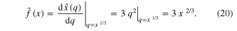
Step 5.
Substitute (19) for R(x) and (20) for  in (12a) to obtain the following Ideal Generic Memristor:
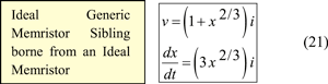
We end section 2 by noting that the hp memristor defined by (5) and (6) on Page 81 of [11] is a trivial form of an Ideal Generic Memristor. In particular, let us rewrite (6) in [11] as follow.

where, 
Applying (14a) to the above expression, we obtain

which is (7) in [11].
Since an Ideal Generic Memristor is mathematically equivalent to an Ideal Memristor, it follows that the Titanium Dioxide hp memristor presented in the seminal 2008 nature paper [11] is an Ideal Memristor.
3. Potassium and sodium ion channels are generic memristors
Figure 15(c) shows the classic Hodgkin–Huxley model [33] of the giant axon of the North Atlantic squid Loligo, shown in figure 15(a). The  modified symbol
  and the
  modified symbol
  are dubbed time-varying potassium conductance and time-varying sodium conductance, respectively, by Hodgkin and Huxley because they were unable to identify the nature of these two peculiar circuit elements which behave like resistors obeying Ohm's law, but whose resistance changes with time. Hodgkin–Huxley's mistaken identity has led to many anomalies such as its implication of a pervasive presence of huge inductors of several Henries throughout the brain [34]. Such anomalies were finally resolved by replacing the potassium and sodium time-varying resistors in figure 15(c) with memristors, as shown in figure 15(d) [35].

Figure 15. Resolution of the anomalies arising from Hodgkin–Huxley incorrect identification of the potassium and sodium ion channels as time-varying resistors. (a) The North Atlantic squid Loligo (b) Axon membrane showing only the postassium and sodium ion channels (c) Hodgkin–Huxley model (d) Revised Hodgkin–Huxley model (e) Characterization of the potassium ion channel as a first-order memristor (f) Characterization of the sodium ion channel as a second-order memristor.
Download figure:
Standard image High-resolution imageIn particular, figure 15(d) shows the time-varying Potassium ion-channel resistor in the Hodgkin–Huxley model is in fact a time-invariant first-order Generic Memristor with  as the state variable, as defined in figure 15(e). Similarly, the time-varying sodium ion-channel resistor is in fact a time-invariant second-order Generic Memristor, as defined in figure 15(f).
3.1. Pinched hysteresis loops evolve with frequency
Table 5 shows the Lissajoux figure in the iK versus vK plane of the potassium ion-channel memristor for nine different frequencies, as computed from the first-order memristor equations shown in figure 15(e). Observe that at dc (f = 0 Hz), the iK versus vK Lissajoux figure is a single-valued curve. As the excitation frequency f increases, a loop whose lobe area5
 ⩾ 0 in the first quadrant, and Ar− ≦̸ 0 in the third quadrant emerged and increases in magnitude between f = 1 Hz and f = 50 Hz. Thereafter, the magnitude of both lobe areas decreases monotonically from f = 200 Hz to f = 3 KHz. At very high frequencies, the magnitude of both lobe areas decreases to zero, resulting in a straight line through the origin at f = 1 MHz.
Table 5. Lobe area and orientation of the pinched hysteresis loops of the potassium ion-channel memristor for input voltage vK(t) = Asin (2πft) with amplitude A = 50 mV.
 |
To confirm the 'zero phase-shift' signature of memristors, the sinusoidal input voltage waveform (in red color) vK(t) and the corresponding periodic current waveform iK(t) (in blue color) are plotted on the same set of axes in figures 16(a)–(c) for three frequencies f = 10 Hz, 50 Hz, and 200 Hz, respectively. Observe that iK(t) = 0 whenever vK(t) = 0, as expected.

Figure 16. Potassium current  and input sinusoidal voltage
  A = 50 mV, for three frequencies (a) f = 10 Hz (b) f = 50 Hz, and (c) f = 200 Hz.
Download figure:
Standard image High-resolution imageTable 6 shows the Lissajoux figure in the iNa versus vNa plane of the Sodium ion-channel memristor for nine different frequencies, as computed from the second-order memristor equations shown in figure 15(f). Again, the iNa versus vNa Lissajoux figure at dc (f = 0 Hz) is a single-valued curve. As the frequency increases, a pinched hysteresis loop with magnitude of lobe area Ar+ in the first quadrant, and magnitude of lobe area Ar− in the third quadrant emerged and increases from f = 1 Hz to f = 50 Hz. Beyond this frequency, the magnitude of both lobe area decreases monotonically until it collapses into a straight line through the origin at f = 1 MHz.
Table 6. Lobe area and orientation of the pinched hysteresis loops of the sodium ion-channel memristor for input voltage vNa (t) = Asin (2πft) with amplitude A = 120 mV.
 |
Figure 17 shows the waveform pairs (v(t), i(t)) plotted on the same pair of axes at f = 50 Hz, 200 Hz, and 500 Hz. Again, we observe iNa(t) = 0 whenever vNa(t) = 0, thereby confirming that it too exhibits the memristor 'zero-phase-shift' signature.

Figure 17. Sodium current  and input sinusoidal voltage
  A = 120 mV, for three frequencies (a) f = 50 Hz (b) f = 200 Hz, and (c) f = 500 Hz.
Download figure:
Standard image High-resolution imageIt is important to understand that the Pinched hysteresis loops associated with a particular memristor depend not only on the amplitude and frequency of the sinusoidal voltage waveform applied across the memristor, but also on the choice of the waveforms as well, as clearly demonstrated as a function of frequency, and at dc (not sinusoidal), in table 5 for the potassium ion-channel memristors, and table 6 for the sodium ion-channel memristor. In other words, pinched hysteresis loops are not models because 'models must predict' [37, 38], and pinched hysteresis loops can not predict what happens if another waveform is applied across the device.
But pinched hysteresis loops measured from a device certifies that device is a memristor. Whether it is an Extended Memristor, a Generic Memristor, an Ideal Generic Memristor, or an Ideal Memristor, can be easily tested by additional properties manifested by different classes of memristors to be presented in the following sections.
A fundamental property of pinched hysteresis loops measured from a particular memristor is that it is an 'identity card' of that device. Apply the same input voltage waveform and the same pinched hysteresis loop must emerge. As a futuristic application, imagine every person has a catalog of 'healthy' pinched hysteresis loops measured from his potassium and sodium ion channels, as well as several other life-depending voltage-gated ion channels, such as calcium and chloride ion channels [40]. Since such 'healthy' pinched hysteresis loop fingerprints will change shape when a person developed an ion-channel disease6 [40] later in life, such ion-channel disease could conceivably be detected just by comparing his latest measured pinched hysteresis loops with those retrieved from his healthy ion-channel data base.
3.2. Pinched hysteresis loops degenerate to straight lines at high frequencies
As illustrated in table 5, the pinched hysteresis loops associated with the potassium ion-channel memristor degenerates to a straight line for frequencies f > 1 MHz. Similarly, table 6 shows the pinched hysteresis loops of the sodium ion-channel memristor also degenerates to a straight line for frequencies f > 1 MHz. Such unique phenomenon must emerge at sufficiently high frequencies for all Generic Memristors as proved in page 212 of [42]. The same method of proof can be used to prove that for Extended Memristors (where the memristance function  , or memductance function
  , depend not only on the state variable
  , but also on the input current i or voltage v, respectively), their pinched hysteresis loops must degenerate to a single-valued V–I curve resembling those measured from nonlinear resistors [3]. Since this phenomenon can occur only if the memristor is an Extended Memristor, it can be used to determine whether a memristor is a Generic Memristor (with linear v–i relationship) or an Extended Memristor (with single-valued nonlinear v–i relationship) at high frequencies.
Another peculiar aspect of the limiting behavior of Generic Memristors at high frequencies is that the slope of the limiting straight lines is not constant, but changes with the amplitude A of the sinusoidal input voltage v(t) = A sin ωt, as illustrated in figure 18 for the potassium memristor defined in figure 15(e), and in figure 19 for the sodium memristor defined in figure 15(f).

Figure 18. Limiting behaviors of Generic Memristors at high frequencies. (a) slope (memductance G(vK )) of limiting straight lines for Potassium memristor for amplitude A = 40, 50, and 60 mV. (b) Potassium Memductance G(vK ) at high frequencies calculated by two different methods [42].
Download figure:
Standard image High-resolution image
Figure 19. Limiting behaviors of Generic Memristors at high frequencies. (a) slope (memductance G(vNa) of limiting straight lines for sodium memristor for amplitude A = 130, 140, and 150 mV. (b) Sodium Memductance G(vNa) at high frequencies calculated by two different methods [43].
Download figure:
Standard image High-resolution image3.3. dc V–I curves
The potassium ion-channel memristor defined in figure 15(e) is an example of a Generic Memristor described by one state equation; namely,


where we have changed the potassium ion channel 'gate activation' variable 'n' to the symbol 'x' used in this paper. Equating (23) to zero and solving for the dc equilibrium point as a function of the applied dc voltage vK = VK, we obtain [43]:

Substituting (24) for x in (22), we obtain the dc VK–IK curve shown in figure 20 for the potassium ion-channel memristor.

Figure 20. The potassium ion-channel memristor dc VK–IK curve. The inset shows the enlargement over 0 ≦̸ VK ≦̸ 50 mV.
Download figure:
Standard image High-resolution imageThe sodium ion-channel memristor defined in figure 15(f) is an example of a Generic Memristor described by two state equations; namely,


where we have changed the sodium ion channel 'gate activation' variable 'm' to the symbol 'x1' and the 'gate inactivation' variable 'h' to the symbol 'x2', respectively, to be consistent with our notations in this paper. Equating (26) and (27) to zero and solving for the dc equilibrium point as a function of the applied dc voltage vNa = VNa, we obtain [43]:


Substituting (28) and (29) for x1 and x2 in (25), we obtain the dc VNa–INa curve shown in figure 21 for the sodium ion-channel memristor. Observe that at the dc steady state regime, the potassium ion-channel is equivalent to a nonlinear resistor described by the dc VK–IK curve shown in figure 20 [37]. Likewise, at dc steady state, the sodium ion-channel memristor is equivalent to a nonlinear resistor described by the dc VNa–INa curve shown in figure 21.

Figure 21. The sodium ion-channel memristor dc VNa–INa curve. The inset shows the enlargement over −100 mV ≦̸ VNa ≦̸ 50 mV.
Download figure:
Standard image High-resolution imageIn other words, Generic Memristors, in general, behave just like a nonlinear resistor under the dc regime7 .
4. Ideal memristors have bizarre dc V–I curves
Following is a high-school level physics question which most memristor researchers do not know the answer but are afraid to ask:
What happens when one connects a battery directly across a memristor8 ?
The answer is: In most cases, one sees either a two-segment piecewise-linear (PWL) V–I curve, or smoke!
The following simple example illustrates why.
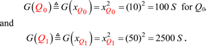
4.1. Example 1: Ideal memristor with a dc V–I 'Rectifier' curve
Consider the three-segment PWL q versus φ curve (along with its equation) of an Ideal Memristor as shown in figure 22(a). It's memductance  is shown in figure 22(b). Suppose we connect a Battery with voltage of E volts across this memristor at t = 0. Assuming
  , the voltage waveform v(t) and flux waveform
  are shown in figure 23(a) for E > 0, and in figure 23(b) for E < 0. Observe that in either case,
  never stops, but increases to +∞ if E > 0, and to −∞ if E < 0. Hence, in theory, an Ideal memristor is never in equilibrium when connected to a battery. However, since the last two segments of the q versus φ curve in figure 22 are straight lines, after a sufficiently long time interval for the flux
  to travel from
  in figure 22(a) to the breakpoint located at
  , if E > 0 (resp., to the breakpoint located at
  if E < 0), the memristor is equivalent (at dc) to a ¼ Ω (4 Siemens) resistor if E > 0 (resp., 2 Ω resistor if E < 0). Consequently, one would measure the rectifier-like dc V–I curve shown in figure 23(c). In this case, the Ideal Memristor defined in figure 22 has indeed a dc V–I curve in the sense that given any dc voltage v = E, this V–I curve would predict the corresponding dc current i = I, in accordance with figure 23(c), namely9
,
if E < 0), the memristor is equivalent (at dc) to a ¼ Ω (4 Siemens) resistor if E > 0 (resp., 2 Ω resistor if E < 0). Consequently, one would measure the rectifier-like dc V–I curve shown in figure 23(c). In this case, the Ideal Memristor defined in figure 22 has indeed a dc V–I curve in the sense that given any dc voltage v = E, this V–I curve would predict the corresponding dc current i = I, in accordance with figure 23(c), namely9
,

for all t > T, where  is the time it takes to move from
  to
to  along the PWL q versus φ curve in figure 22(a).

Figure 22. The ideal memristor for example 1. (a) three-Segment PWL q versus φ curve. (b) The 'Stair case' memductance G(φ) associated with (a). The height of each step is equal to the slope of the corresponding segment.
Download figure:
Standard image High-resolution image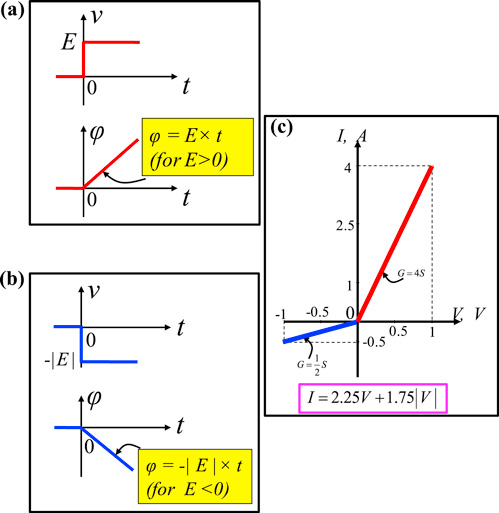
Figure 23. The dc V–I curve of the ideal memristor defined in figure 22 is a two-segment PWL rectifier-like curve.
Download figure:
Standard image High-resolution imageWe end this subsection by commenting that if the φ versus q curve of an ideal memristor tends to a straight line with slope R1 for large positive values of φ, and slope R2 ≪⃒ R1 for large negative values of φ, regardless of the shape of the q versus φ curve between the two extreme straight-lines, then we may say that it has a dc V–I curve, as shown in figure 24, provided we understand that in term of the state variable φ, the memristor is in reality never in a steady-state regime since  .
.

Figure 24. An ideal memristor with a linear q versus φ characteristic for large positive and negative values of φ has a rectifier-like dc V–I curve.
Download figure:
Standard image High-resolution image4.2. Example 2: Ideal memristor without a dc V–I curve
Consider an Ideal Memristor defined by

The memductance is given by

Applying an E-Volt battery across this memristor as in figure 22, we obtain the same  shown in figure 23(a) for E > 0 and figure 23(b) for E < 0. The current i(t) in this case is

It follows from (33) that this Ideal Memristor never settles down to a dc current when connected to a battery of either polarity, and hence it does not have a dc V–I curve!
Observe that in practice, such an Ideal Memristor would burnt-out long before its current gets too large. The moral of this example is that one should never connect a battery directly across an Ideal Memristor characterized by a monotonically-increasing 'polynomial' q versus φ curve, because the memductance G(t) = E3 × t2 would quickly lead to the destruction of the device. It follows therefore that a sufficiently large resistor should always be connected in series with the battery so that the maximum current would be limited to E/R in the event that the memristor tends to a short circuit, in the worst case, after some finite time.
4.3. The dc V–I curve of an ideal memristor is a single point (V, I) = (0, 0)!
From a rigorous circuit-theoretic perspective, an Ideal Memristor has a dc V–I curve consisting of only one point, namely, the origin (V, I) = (0, 0)10 . This may look weird but it is correct. It also makes sense because no matter how small a dc voltage source, or dc current source, that one applies across an ideal memristor, it's associated flux, or charge is a ramp signal heading for infinity, and the memristor will never be at rest, and hence no other point in the V–I plane of an Ideal Memristor will ever be at a dc steady state.
The above memristive Nullator phenomenon is in fact the explanation for why one never sees from among the hundreds of papers published on memristors, a single dc V–I curve. It just does not exist11 .
But this somewhat unexciting result is precisely the hallmark of an Ideal Memristor. If one fails to trace a dc V–I curve of a memristive device (i.e., a device endowed with pinched hysteresis loops in the v–i plane), because it keeps burning out, then that device is an Ideal Memristor!
5. Ideal memristor: four guided tours
Since most ideal memristors, and their Ideal Generic Memristor siblings, do not have a dc V–I curve, the best graphical interpretation for such pristine memristors is via their φ versus q constitutive relation, and pinched hysteresis loops, as shown in figure 25. It is illuminating to interpret the slope at each point  on the φ versus q curve in figure 25(a) as the memristance R(q(t)) of the memristor at
  , seen as a 'snap shot' at time t. The 'snap shot' of the corresponding point on the associated pinched hysteresis loop taken at the same instant of time t is shown in figure 25(b). The slope of the straight line joining the origin and this point is called the chord resistance at time t. Observe that the slope at
  in figure 25(a) is equal to the slope of the corresponding chord resistance, measured at the same instant of time. The memristance is the analog of the so-called 'small-signal' resistance, at a dc bias point in electronic devices [3, 45].

Figure 25. (a) A typical φ versus q constitutive relation of an ideal memristor. (b) A typical pinched hysteresis loop, traced with a normalized sinusoidal current source i(t) = sin t. For an ideal memristor, the small-signal resistance Rm (t) and the chord resistance R(t) are equal at the same instants of time.
Download figure:
Standard image High-resolution imageObserve that whereas the point  moves along the φ versus q curve in figure 25(a), its associated chord resistance is pinned down at the origin. It is often enlightening to imagine that as one traces the tip of 'the chord resistance' vector over the first half period 0 ≦̸ t≦̸ π along the pinched hysteresis loop in figure 25(b), the corresponding point
  in figure 25(a) must track along the φ versus q curve so that their slopes are equal at all times. Since q(t) for the second half period due to i(t) = sin t merely retraces the φ versus q curve, it follows that the associated pinched hysteresis loop in the 3rd quadrant in the v–i plane must be an odd-symmetric image of the hysteresis lobe in the 1st quadrant. In other words, pinched hysteresis loops traced with a sinusoidal input current i(t) = A sin ωt (resp., sinusoidal input voltage v(t) = A sin ωt) are odd-symmetric.
To develop a good intuition at analyzing a pinched hysteresis loop measured from a real two-terminal device, we present below three guided tours using the same ideal memristor q versus φ curve defined by the following three segment PWL equation12 :

Choosing a PWL curve allows us to calculate all waveforms v(t), φ(t), q(t), i(t), and R(t) analytically, via simple closed form formulas. Moreover, the pinched hysteresis loop associated with any PWL φ versus q curve will also be piecewise-smooth functions, with an abrupt 'jump transition' whenever φ(t) arrives at a breakpoint, when the slope (i.e., the memristance R) changes suddenly.
5.1. Ideal memristor guided tour 1
Consider applying a sinusoidal voltage v(t) = 0.8 sin t across an Ideal Memristor with the three segment PWL q versus φ curve shown in figure 26. Assuming an initial flux  and using the analytical formula (34), we obtain the corresponding charge q(t) and current i(t), as well as, the memductance G(t), shown as vertically-aligned waveforms in the left column of figure 26. The loci corresponding to
  starts from the initial point
  and move along the leftmost blue line segment until it reaches the first breakpoint
  at
at  , where it changes slope and moves upward along route
  , passing the origin, and continue its upward motion along route
  , until it arrives at the second breakpoint
  at
at  , whereupon it turns but continues moving rightward along route
  where the corresponding voltage v(t) reaches approximately its peak. Observe, however,
  must continue to increase until point
  at
at  , where it begins its return journey, along the same route
  . Somewhere around the midpoint of route
  , the loci crosses over the origin in the v–i plane, but still travelling leftward until it returns to point
  (relabelled as point
  ), and continues its return trip downward along route
  , (relabeled as route
  ). Eventually, it will arrive at point
  (relabelled as
  ), and continues its leftward odyssey until it returns to the starting point
  φ(0) = −0.4, at t = 2π.

Figure 26. Ideal Memristor Guided Tour 1. The input is a sinusoidal voltage v(t) = A sin t with A = 0.8. The initial flux is chosen at  .
.
Download figure:
Standard image High-resolution imageThe pinched hysteresis loop associated with the above odyssey can be easily constructed as shown in the red loci on top of the right column in figure 26. Observe that the four abrupt jumps in i(t) occur at the four time instants where one of the two breakpoints  and
and  is crossed. Observe also the slope of the lowermost and uppermost loci is equal to the slope of the middle segment
  (resp.,
  ) of the q versus φ curve. Observe also the slope of the near-horizontal line in the red v–i curve is equal to the slope of the leftmost (resp., rightmost) segment of the q versus φ curve.
5.2. Ideal memristor guided tour 2
Consider next a variant of tour 1 where the only change is the initial state, namely, from  to
to  . The resulting tour map in figure 27 is virtually identical, except for the two double-arrowhead tails that stick out at the extremities. This new feature is important because many published pinched hysteresis loops exhibited similar tails [47].

Figure 27. Ideal Memristor Guided Tour 2. This tour differs from Tour 1 only by changing the initial state from  to
to  a mere 0.10 increase in φ(0). Observe the two red tails that emerged at the loci's extremities.
Download figure:
Standard image High-resolution image5.3. Ideal memristor guided tour 3
Our next tour is a slight variant of tour 2 where we only increase the initial state from  to
to  a further tiny increase in
  of only 0.05. The resulting pinched hysteresis loop is shown in figure 28. Observe the dramatic change in the shape of the pinched hysteresis loop from a trapezoidal lobe to a triangular lobe! Such triangular-lobe features can also be found in many published papers [47, 48]. We can not overemphasize that the same memristive device can exhibit drastically different pinched hysteresis loops with the same applied input voltage by tuning only the initial state.

Figure 28. Ideal Memristor Guided Tour 3. This tour differs from Tour 2 only by changing the initial state from  to
to  , a mere 0.05 increase in
  . Observe the dramatic change in shape from a trapezoidal to a triangular lobe.
Download figure:
Standard image High-resolution image5.4. Ideal memristor guided tour 4
Notice that all of the pinched hysteresis loops we have observed from the same Ideal Memristor in figures 26– 28 are odd symmetric, as expected from all Ideal memristors. Just in case the reader may attribute this odd symmetry property as resulting from the odd symmetry of both the excitation waveform v = A sin t, and that of the q versus φ curve, our final tour changes this odd-symmetric constitutive relation to the non-symmetric q versus φ curve in figure 29. The resulting pinched hysteresis loop is seen to retain its odd-symmetry property, as expected of all Ideal Memristors [62].

Figure 29. Ideal Memristor Guided Tour 4 with a non-symmetric q versus φ curve. Observe the pinched hysteresis loop is odd symmetric, as predicted.
Download figure:
Standard image High-resolution image5.5. All ideal memristors are non-volatile analog memories
In the semiconductor device parlance, a 'non-volatile' analog memory means a memory device that can store a continuous range of resistance values, and in which the stored data is preserved even after the electrical power is switched off from the system where the memory device is embedded. This class of memory devices is distinct from conventional non-volatile 'binary' memories where only the '0' state and '1' state can be stored. The main applications of non-volatile analog memories are for mimicking 'synapses' whose weight can be continuously tuned for 'learning' in intelligent brain-like machines [35].
Since the state equation defining an Ideal Memristor is

for voltage-controlled Ideal memristors, and

for current-controlled Ideal memristors, switching off the power means setting both the memristor voltage v, and the memristor current i, to zero. In both cases,
where  and
and  are 'any' real number that
  and
and  assumes at
  , assuming the power is switched off at t = 0.
It follows that an Ideal Memristor is endowed with the capability to store any real number R,

(in the form of a resistance, or a conductance), and retaining it for eternity without a power supply, at least in principle.
Since not all memristors are non-volatile memories, we end this section by calling attention to this very special virtue of an ideal memristor and its siblings:

5.6. Modelling Beck et al 'Bow-Tie' loop
We end this section by tuning the three parameters of a three-segment PWL q versus φ curve to obtain an Ideal Memristor that exhibit virtually the same well-known Bow-Tie shape pinched hysteresis loop presented in [14]. The red horizontal segment in the lower left column of figure 30(a) is most likely an artifact of an artificially imposed 'Compliance current' from the measuring instrument. For pedagogical reasons, the waveforms  ,
,  and i(t) are presented in figure 31, along with the triangular-lobe pinched hysteresis loop.

Figure 30. The Ideal Memristor defined by the three-segment PWL q versus φ curve in (c) gives a bow-tie shape pinched hysteresis loop for a sinusoidal input voltage v(t) = 0.75 sin t in (b), which matches approximately the measured curve (a) presented in [14].
Download figure:
Standard image High-resolution image
Figure 31. The waveforms of  ,
,  and i(t) resulting from applying a sinusoidal voltage v(t) = 0.7 sin t across an Ideal Memristor with a three-segment odd-symmetric PWL q versus φ curve (shown in figure 30(c)).
Download figure:
Standard image High-resolution imageWe wish to point out that there is a qualitative difference between Beck's pinched hysteresis loop in figure 30(a) and that predicted from the ideal memristor q versus φ curve in figure 30(c), namely, the v–i curve switches from a high-resistance state (the near-horizontal branch) to a low-resistance state at approximately v = −0.5 V, before the sinusoidal input switching signal had reached its most negative value. This discrepancy (assuming Beck's pinched hysteresis loop in figure 30(a) represents true real-time measurements and not an artifact of the measuring instrument) suggests that a generic or even an extended memristor may be needed to emulate Beck's pinched hysteresis loop more accurately.
6. Generic memristor: a guided walk
Consider the hypothetical Generic Memristor defined in figure 32, namely

Figure 32. A hypothetical Generic Memristor. The top part shows its dc V–I curve in a small neighborhood of v = 0 consisting of two crossing straight lines. The lower PWL curve is defined by f(x).
Download figure:
Standard image High-resolution imageState-Dependent Ohm's Law:

where

State-Equation:

where

is the exact equation of the three-segment PWL curve shown in the bottom of figure 32.
6.1. Non-volatile binary memory
When v = 0, the state equation reduces to

which is best analyzed in the  versus x plane shown in figure 32, where the vertical axis represents the rate of change
  of the state variable x. Observe that
  at any point on the
  curve that lies above the x-axis. This means that the motion through each point on f(x) above the x-axis must move to the right as time increases, as depicted by three arrowheads pointing to the right. Similarly, since
  below the x-axis, any point on f(x) lying below the x-axis must move to the left as time increases, as depicted by the three arrowheads pointing to the left.
Observe that at the three points  ,
,  and
and  where f(x) = 0,
  . This means that if the initial state is located at one of these three points, there will be no motion at all. This is why
  ,
,  and
and  are called an equilibrium point of this memristor when v = 0 (power is switched off).
A cursory inspection of the  f(x) and the arrowheads indicating the direction of motion near each of the three equilibrium points shows that
  is an unstable equilibrium, and hence any initial state different from the three equilibrium points must move either to
  if x(0) < 30, or
  if x(0) > 30. In the theory of nonlinear dynamics [3, 49], the equilibrium point
  is said to be an attractor with a basin of attraction consisting of the open interval x < 30 because any initial point x(0) lying within this interval is attracted to
  . Similarly, the equilibrium point
  is said to be an attractor with a basin of attraction consisting of the open interval x > 30. In the parlance of nonlinear circuit theory, any curve f(x) plotted in the
  versus x plane, along with arrowheads pointing the direction of motion from representative points, is called a dynamic route [3, 45]. In spite of its simplicity, the dynamic route is the most powerful and useful tool for analyzing the dynamics of any first-order differential equation
  because one can predict how any initial state will evolve with increasing time. For example, the dynamic route (for v = 0) in figure 32 implies that this memristor must assume one of two possible stable states
  and
and  with the power switched off. This means that this memristor is a non-volatile (because v = 0) 'binary memory', whose small-signal conductance
  measured in a small neighborhood of each asymptotically stable [3, 45] equilibrium point Q defines the slope of a straight line through the origin (v = 0) whose equation is precisely Ohm's law. Since this memristor has two asymptotically stable equilibrium points
  and
and  , the two corresponding memductances are given by
The above trivial calculations are summarized by two crossing straight lines with slope G0 and G1, respectively, in figure 32. It is traditional to call state  the off state '0' because it is associated with a significantly higher resistance (or equivalently, smaller conductance). Similarly, the state
  is called the on state '1' because it is associated with a significantly lower resistance.
Our next task is to find a way to set the memristor by switching from a high-resistance state  to its low resistance state
  . Conversely, we must also find a way to reset the memristor by switching from a low resistance state
  to a high resistance state
  .
.
6.2. How to set and reset memory states?
The conceptually simplest way to switch (i.e., set) from the high-resistance (low conductance) state  to the low resistance (high conductance) state
  is to apply a square pulse of appropriate pulse width Δt, and pulse amplitude A, as shown in the upper part of figure 33. An application of a 15 V square pulse is equivalent to translating
  f(x) upwards by 15 units, as shown by the
  . The dynamic route starting from
  at t = 0− would jump abruptly from
  to a point directly above
  on the
  at t = 0+. Since the
  is located above the x-axis over the range of interest, its motion can only move to the right, until time t = Δt, where the square pulse returns to zero, and the
  reverts back abruptly to the
  , where upon the dynamics must continue to move along the dynamic route indicated by the two black arrowheads, until it converges to the low-resistance memory state
  .
.

Figure 33. Dynamic route associated with the set operation is shown on top. The dynamic route associated with the reset operation is shown below.
Download figure:
Standard image High-resolution imageSwitching back (i.e., reset) from the low-resistance (high conductance) state  to the high-resistance (low conductance) state
  consists of simply applying a negative voltage pulse, as shown in the lower part of figure 33.
6.3. Why minimum pulse width and minimum pulse amplitude?
The top part of figure 34 shows the dynamic route resulting from a too-short pulse width Δt. Observe the return downward jump falls on the negative side of the  , whose dynamic route demands that motion must move to the left, eventually returning to
  . Hence the switching process had failed in this case. It is clear from the upper diagram that to switch from
  to
to  successfully, the pulse width Δt must be at least long enough for the downward jump to land to the right of the unstable equilibrium point
  , as in figure 33 (top).

Figure 34. (a) The dynamic route in the top diagram predicts switching failure due to an insufficient pulse width Δt. (b) The dynamic route at the bottom diagram predicts switching failure due to an insufficient pulse amplitude A.
Download figure:
Standard image High-resolution imageThe lower part of figure 34 shows the dynamic route resulting from a too-small pulse amplitude A. Observe the return downward jump will fall on the negative side of the  , where the dynamic route decreed that the motion must be to the left, thereby returning to the initial point
  . Observe that this scenario will take place no matter how large the pulse width is because it would take an infinite amount of time for the motion along the
  to reach x = 15 because the point at x = 15 (see inset) is a new equilibrium point while the square pulse is on, and it would take an infinite amount of time to arrive at an equilibrium point [3, 49]. For a successful switching from
  to
to  , the pulse amplitude A must be at least equal to 10 in order for the minima of the
  to stay above x-axis, as in figure 33 (top).
6.4. A bi-continuum non-volatile memory
Consider the Generic current-controlled memristor defined in figure 35, where the seven-segment PWL function f(x) for the memristor state equation shown in the bottom has an explicit formula (see appendix) shown on top. To focus on the dynamic nature of the non-volatile memory exhibited by this memristor, we had deliberately left the memristance R(x) unspecified to emphasize that, R(x) is irrelevant to the characterization of the memristor's non-volatility. The dynamic route at the bottom of figure 35 shows that this memristor is endowed with two disconnected closed intervals of stable (but not asymptotically stable) equilibrium points; namely x  [−2, −1] on the left of the origin, and x
  [1, 2] on the right. Every point belonging to either interval is a member of an entire continuum of non-volatile memory states because
  for i = 0, and for any x belonging to either intervals where f(x) = 0. Observe that in contrast to ideal memristors where the entire x-axis is a non-volatile memory state, here we have two closed intervals of memory states. Which of the two intervals should be assigned an 'off' state, or an 'on' state, depends on how we define the memristance function R(x). It follows from the above analysis that the continuum non-volatility property of a memristor depends only on the closed interval of x where f(x) = 0, when i = I = 0.

Figure 35. A non-volatile memristor whose memory states reside on two disconnected closed intervals where f(x) = 0.
Download figure:
Standard image High-resolution image6.5. Pinched hysteresis loop need not be symmetric
We have proved in section 5 that the pinched hysteresis loop of any Ideal Memristor, or its Ideal Generic Siblings, must necessarily be odd-symmetric for a sinusoidal input voltage or current. The four pinched hysteresis loops shown in figures 36(a)–(d) for the Generic Memristor defined in (35)-(36) and figure 32 (for four different values of the amplitude A) show that they are not symmetric. To analyze the source of the non-symmetry, figures 37 and 38 show the waveforms of v(t), i(t) and G(t), aligned vertically in time. A careful analysis and comparison with corresponding waveforms associated with Ideal Memristors reveals that whereas both the voltage v(t) and current i(t) of Ideal Memristors exhibit a reflected half-wave symmetry where the negative of the waveform during the second-half period of v(t) are mirror images of each other (See the left column of figures 26– 29, and 31), those shown in figures 37 and 38 do not exhibit such reflected half-wave symmetry. It follows that whenever a pinched hysteresis loop measured from a memristive device is not odd-symmetric then that device can not be an Ideal Memristor.
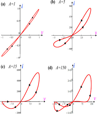
Figure 36. Four not-symmetric pinched hysteresis loops associated with the Generic Memristor in figure 32.
Download figure:
Standard image High-resolution image
Figure 37. Waveforms of v(t), i(t), G(t) and their associated unsymmetric pinched hysteresis loops for sinusoidal voltage input with amplitude A = 5.
Download figure:
Standard image High-resolution image
Figure 38. Waveforms of v(t), i(t), G(t), and their associated unsymmetric pinched hysteresis loops, for sinusoidal voltage input with amplitude A = 15.
Download figure:
Standard image High-resolution image7. Extended memristors: a glimpse
Consider the Extended Memristor defined in figure 39:
Extended Ohm's Law


Figure 39. An Extended Memristor and its dc V–I curve, which consists of three disconnected branches described by the unstable branch V = 0 (dotted red loci), and two asymptotically-stable branches (for each fixed value of I) defined analytically in blue for x(0) > 0, and in red for x(0) < 0.
Download figure:
Standard image High-resolution imagewhere

State Equation

where

Let us derive the dc V–I curve by substituting i = I in (39b ) and solve the dc equilibrium equation
It follows from (40) that x = 0 is an equilibrium state of the Extended Memristor for all dc current I. The remaining 2 roots of (40) are solutions of

The solution of the quadratic equation (41) can be derived explicitly and when substituted into (38), we obtain the following two disconnected V–I curve branches:


The three dc V–I curve branches are shown in figure 39. We will show below that the dotted red branch V = 0 is an unstable dc V–I curve and hence not observable. Likewise, the other two branches will be shown to be asymptotically stable and hence can be easily observed by choosing appropriate initial states x(0).
Let us investigate the stability of the 3 dc V–I curves. Consider the non-volatile case where I = 0. The corresponding state equation determining the dynamics in this case is obtained by substituting i = 0 in (39b ):

The dynamic route associated with the state equation (43) is shown in figure 40. Observe that the equilibrium state x = 0 is unstable as expected. The equilibrium state x = 1 is asymptotically stable with a basin of attraction defined by x(0) > 0. The equilibrium state x = −3 is also asymptotically stable with a basin of attraction defined by x(0) < 0.

Figure 40. Dynamic route of Extended Memristor when i = I = 0.
Download figure:
Standard image High-resolution imageFor non-zero values of I, the corresponding dynamic routes give exactly the same basin of attractions as in the non-volatile case. The above analytical results are summarized in figure 40.
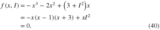
It remains for us to examine the pinched hysteresis loop of this Extended Memristor. Figure 41 shows four pinched hysteresis loops for four frequencies f = 0 Hz, 10 Hz, 50 Hz, and 200 Hz, for i = 10 sin (2πft), and initial state x(0) = 6.3. As expected the pinched loop shrinks as the frequency f increases. Observe, however, that the limiting Lissajoux figure at high frequencies does not tend to a straight line but to a single-valued curve (magenta)13 . Since the limiting Lissajoux figure for Generic Memristors at very high frequencies is always a straight line whose slope varies with the input signal waveforms, the emergence of a single-valued curve in the V–I plane is the exclusive property of all Extended Memristors. We can therefore use this fingerprint to identify whether a set of experimental pinched hysteresis loop pertain to a Generic Memristor, or to an Extended Memristor.

Figure 41. The two lobe areas of the pinched hysteresis loop of the Extended Memristor decreases as the frequency increases, and at very high frequencies, the pinched hysteresis loops tend to a single-valued nonlinear function.
Download figure:
Standard image High-resolution imageWe end this section by showing two different pinched hysteresis loops in figure 42(a) calculated from (38)–(39) for the same input i = 10 sin (2πft), at the same frequency f = 10 Hz, but different initial states x(0) = 6.3 and x(0) = −6.3 respectively. As the frequency increases to f = 200 Hz, the limiting single-valued curves shown in figure 42(b) are also different. This observation is not surprising because even at dc, we have seen two distinct dc V–I curves in figure 39 each having its own basin of attraction. Certainly there must be multiple hysteresis loops as well, each having its own basin of attraction.
Figure 42. For the same input signal waveform different pinched hysteresis loops emerged from the Extended Memristor in figure 39, from different initial states. (a) Distinct pinched hysteresis loops for two initial states x(0) = 6.3, and x(0) = −6.3. (b) Two distinct limiting single-valued curves emerged from x(0) = 6.3 and x(0) = −6.3 at f = 200 Hz.
Download figure:
Standard image High-resolution image8. Locally-active memristors
There are new and often exotic functionalities and applications that call for locally-active memristors, which is defined to be any memristor that exhibits a negative memductance  , or a negative memristance
  , for at least some value of the memristor voltage v, or memristor current i. We have already seen an example of a real operational locally-active memristor in figure 4 ( redrawn from the original 1971 paper [1]) where the q versus φ curve has a negative slope in the region near the origin. Observe that the circuit inside the red black-box contains transistors and operational amplifiers (op amps), which require a power supply to bias them at a dc operating point lying within the device's locally-active domain.
8.1. A locally-active memristor oscillator
Figure 43 shows a simple two-memristor circuit made of a battery and two voltage-controlled Generic memristors called PTC (positive temperature coefficient) thermistor and NTC (negative temperature coefficient) thermistor, respectively. The PTC thermistor is defined by:
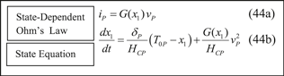
where  ,
,  and
and  are device parameters. It follows from (44) that the PTC thermistor is a 1st- order Generic Memristor with state variable
  , where
  denotes the body temperature of the PTC thermistor. Its dc V–I curve is shown in the inset of figure 43(a). The negative slope in this dc V–I curve implies the PTC thermistor is a locally active Generic memristor with the memductance given by


Figure 43. A two-thermistor Memristor Oscillator (a) connecting a battery across two thermistors makes an oscillator. (b) Voltage waveform VP (t) across the PTC-thermistor memristor (c) Voltage waverform VN (t) across the NTC-thermistor memristor. The initial states are x1(0) = 300 and x2(0) = 300.
Download figure:
Standard image High-resolution imageThe NTC thermistor is defined by:
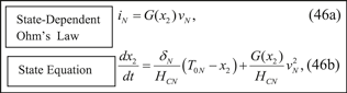
where,
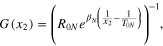
and  ,
,  ,
,  ,
,  and
and  are device parameters. It follows from (46) that the NTC thermistor is a 1st- order Generic Memristor with
  , where
  denotes the body temperature of the NTC memristor.
When a battery is connected across the two-memristor circuit in figure 43(a), a computer simulation of the two differential equations [50] gives the periodic waveform VP (t) of the PTC thermistor voltage shown in figure 43(b), and the periodic waveform VN(t) of the NTC thermistor voltage shown in figure 43(c). The experimental set-up for figure 43(a) was first demonstrated by Reenstra [50] where he had shown the first electronic circuit that oscillates without using an inductor, a capacitor, or a transistor. Here we identify the PTC thermistor to be the locally-active memristor which is responsible for achieving the oscillation without using any energy-storage elements, or other locally-active devices.
8.2. A one-memristor chaos generator
Consider the locally-active current-controlled Generic Memristor defined by
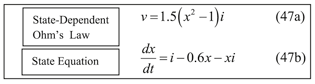
The electronic circuit realization14
in figure 44(a) (inside the red black box) is made of off-the-shelf electronic circuit components [51]. Since the memristance  shown in figure 44(b) is negative for
  , this memristor is locally active, meaning that it can never be built without an internal power supply, such as a solar cell (with a small sunlight-seeking window), radioactive cell, or just a battery. The dc V–I curve of this memristor can be easily derived by setting
  in the memristor state equation (47b) in figure 45(a) to zero, and solving for x as a function of i; namely,


Figure 44. The black box (with the magenta color frame) in (a) contains an electronic circuit made from off-the-shelf components. When measured across the two external terminals on the left, the two-terminal black box is indistinguishable (in principle) from a locally-active memristor whose memristance  is shown in (b). The dc V–I curve measured across the two-terminal blackbox in (a) as shown in (c) has a region with negative slopes, implying that this memristor is locally active.
Download figure:
Standard image High-resolution image
Figure 45. Only three circuit elements are needed to build a chaotic circuit if the nonlinear element is a locally-active memristor, as in figure 44(a). Figure (a) shows the simplest possible chaotic circuit where the equation describes a Generic Memristor with memristance 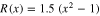 .
.
Download figure:
Standard image High-resolution imageSubstituting (48) for x in (47a), we obtain the following explicit equation for the dc V–I curve of this memristor:

The dc V–I curve measured from the red black box in figure 44(a) is shown in figure 44(c). Again, the local activity accolate bestowed upon this memristor implies that it requires a dc power supply.
When the locally-active Generic memristor is connected in series with an inductor (L = 3) and a capacitor (C = 1), as shown in figure 45(a), we observe a chaotic voltage waveform vC (t) across the capacitor and a chaotic current waveform iL (t) in the inductor, as shown in the top and bottom part of figure 45(b), respectively.
A projection of iL (t) = iC (t) versus the projection of vC (t) in figure 45(c) shows a strange attractor [52] whose waveforms are not periodic but chaotic oscillations. Another chaotic voltage waveform of vC(t) is shown in figure 45(d) (top) along with its fast Fourier transform confirming that the electrical power corresponding to vC(t) is distributed over a continuous range of frequencies, which is the hallmark of chaotic systems.
8.3. A one-memristor oscillator
Figure 46 shows a very simple circuit made of a battery in series with a resistor and a memristor defined earlier in figure 15(f), namely, the Hodgkin–Huxley sodium ion channel memristor, defined by two differential equations involving two state variables m and h, which we reproduce in figure 46(c) for the reader's convenience. A truncated version of the dc V–I curve of this 2nd-order Generic memristor (shown earlier in figure 21) is shown in figure 46(b). A numerical simulation of the circuit in figure 46(a) reveals the existence of an unstable limit cycle in the m versus h plane, as shown in figure 46(d), along with the periodic waveforms of m(t) and h(t).

Figure 46. A one-memristor circuit derived by deleting the capacitor and the potassium ion channel from the Hodgkin–Huxley circuit model.The parameter values of the remaining elements are chosen to be identical to that given in [33]. The linear resistor gl and the two batteries E(Na) and E(l), as well as the external input current Iext are represented by the Thevenin equivalent circuit [45] consisting of a resistor R and a battery E. (a) One-memristor Oscillator (b) Locally-active dc VNa–INa curve of Hodgkin–Huxley sodium ion-channel memristor (c) Definition of the 2nd order sodium memristor. (d) Oscillation resulting from the circuit in (a). Top: limit cycle, Middle: m(t), Bottom: h(t). The parameters values are  , equilibrium point A:
 are calculated from the load line (current intercept with vNa = 0 at INa = 82.735 47 53 56 19 937 and voltage intercept with iNa = 0, at vNa = 275.784 91 78 53 99 791), and gl
= 0.3 mS is chosen to be equal to the leakage current specified in the Hodgkin–Huxley paper [33, 37].
are calculated from the load line (current intercept with vNa = 0 at INa = 82.735 47 53 56 19 937 and voltage intercept with iNa = 0, at vNa = 275.784 91 78 53 99 791), and gl
= 0.3 mS is chosen to be equal to the leakage current specified in the Hodgkin–Huxley paper [33, 37].
Download figure:
Standard image High-resolution imageObserve that since the series combination of a memristor with a linear resistor is equivalent to another memristor [2], we can replace the resistor R and the Na memristor in figure 46(a) by a single composite 2nd-order memristor defined by the following composite state-depenndent
Ohm's law:

This example represents nature's simplest possible oscillator where an oscillation is generated upon connecting a dc battery across a single two-terminal circuit element defined by the above state-dependent Ohm's law, and a state equation with two state variables m and h, defined in figure 46(c). It can be shown that this oscillation is generated via a sub critical Hopf bifurcation mechanism [59].
9. If it's not pinched it's not a memristor
For our final example, consider the simple Extended Memristor defined by:
Extended Ohm's Law

where

State Equation

where

Let us apply a current source

across this memristor. Assuming initial state x(0) = −1 (52a ) gives

Substituting (54) for x in (51a ), we obtain

The Lissajoux figure in the v–i plane is the unit circle shown in figure 47(a), which is not pinched at the origin (v, i) = (0, 0)!

Figure 47. The anomalous circular and hence not-pinched hysteresis loop in (a) becomes a unit-slope straight line when replotted in the v versus x plane.
Download figure:
Standard image High-resolution imageThe above shocking result seems to suggest that one should accept the notion that not all memristors exhibit the pinched hysteresis loop fingerprint. Unfortunately, this simple resolution of the above anomaly will lead to a logical inconsistency which we will now demonstrate. Observe that if we plot the Lissajoux figure in the v versus x plane instead of the v versus i plane, we would get a single-valued loci without any hysteresis, as shown in figure 47(b). In fact, it follows from (51) and (52) that we can write

which is just the definition of a 1 Farad capacitor! It would certainly be nonsense to call a capacitor a memristor.
The correct resolution of the above anomaly is to realize that

for x ≠ 0, which violates the boundedness condition R(x, 0) ≠ ∞ imposed by definition (1a) of an Extended Memristor. It follows that there is no anomaly after all because (51)–(52) imply q = Cv with C = 1F.
Another misconception among some memristor novice is to confuse an obscure three-terminal electrical gadget called the memistor with the memristor. As clearly explained in [57, 58], the memistor is not a circuit element because it does not have a circuit-theoretic definition that would allow one to write circuit equations when it is imbedded in an electrical circuit. It is essential that for a device to qualify as a memristor, the device must have only two electrical terminals, and that it must exhibit a pinched hysteresis loop in the steady state regime under all periodic voltage and current excitations. The memistor has neither of these two attributes.
10. Concluding remarks
Table 7 shows the Memristor time line dated from at least 500 million years ago where fossil record of Jellyfish has been unearthed. Since all Jellyfish must be endowed with voltage-controlled ion channel memristors needed to generate action potentials, the memristor time line extends from the pre-historic era to the present.
Table 7. Memristor Time Line
 |
Every memristor has a unique set of signatures and fingerprints. The signature is the zero-phase-shift property exhibited in figures 10(d), 16 and 17, where v(t) = 0 whenever i(t) = 0 (for current-controlled memristors), or i(t) = 0 whenever v(t) = 0 (for voltage controlled memristors). This property is true for all times t ⩾ 0, and for all waveforms, regardless of whether they are periodic or not. For example, the blue current waveform in figure 10(d) for the skin 'sweat duct' memristor is not periodic, but it crosses that t-axis whenever the input voltage waveform crosses the t-axis. In this sense, there is no time delay (i.e., no phase shift) between the voltage and the current waveforms. This unique property is responsible for the zero-discharge property of the memristor [54].
Pinched hysteresis loops are the fingerprints of all memristors in the periodic regime (i.e. after all transient waveforms had decayed to zero). Since any two distinct periodic input signals would give distinct pinched hysteresis loops, they are truly fingerprints that can be exploited for applications, such as diagnosis of channelopathy diseases that developed over time due to defective ion-channel memristors.
Since pinched hysteresis loops of ideal memristors, and ideal generic memristors, must be odd symmetric, any non-volatile resistive memory device that exhibits a pinched hysteresis loop that is not odd symmetric, such as those shown in figure 36, must be modeled by either a generic memristor, or an extended memristor.
The dc V–I curve is another property that distinguishes ideal from non-ideal memristors. If a memristor does not have a dc V–I curve in the sense that connecting a battery across the memristor would quickly burn-out and destroy the device, then it is an ideal memristor, or an ideal generic memristor.
In particular, since the memristance (resp., memductance) for an ideal, or ideal generic, passive memristor is a monotonically-increasing function of the state variable q, or  (resp.,
  , or
, or  ), we can conclude that except for the very special case where the
  versus
  curve (resp.,
  versus
  curve) tends to a straight line, or a constant, either the memristance, or memductance, must become infinite. In the former case, connecting a dc current source across the memristor would quickly burn-out the device. In the latter case, connecting a dc battery across the memristor would also destroy the device, as depicted in the Cartoon in figure 48.

Figure 48. Connecting a battery across an 'ideal memristor' whose memductance  increases to infinity as
  increases would quickly end up in smoke!.
Download figure:
Standard image High-resolution imageNot all memristors have non-volatile memories. For example, both the potassium memristor and the sodium memristor are volatile memristors because they both have single-valued dc V–I curves (see tables 5 and table 6) so that the small-signal resistance at the origin (V, I) = (0, 0) is unique.
Not all Non-volatile memristors are locally passive; such locally-active memristors need an internal dc power supply to function properly. For example, the memristor defined by (38)-(39) in section 7 is locally active. This memristor is non-volatile in the sense that even if the power is switched off, it has two distinct dc V–I curves which provides a bistable memory whose state can be sensed by applying a small sensing signal with a dc bias. The internal power supply does not imply that a dc battery is needed, as it may be generated internally via solar, chemical, or nuclear energy sources. It is interesting to note that locally-active non-volatile memristors, such as that cited above, have distinct pinched hysteresis loops, for the same input signal, as depicted in figure 42, for two different initial states.
There are many exotic functionalities that can only be executed by locally-active memristors, such as those presented in section 8. They can be built using locally-active components, such as transistors and op-amps, powered by a dc power supply, as demonstrated in figure 4 and figure 44.
We end this tutorial by stressing that for a device to be called15 a memristor, its hysteresis loop must be pinched and must pass through the origin in the v–i plane. This fundamental condition may not hold for (1) in the definition of an extended memristor unless R( x , 0)≠∞, and G( x , 0)≠∞. The simple example in section 9 is a case in point.
Finally, we note that by a trivial change of symbols, say from (q, φ) to (σ, φ), or (q, ρ) where  and
and  , one can define memcapacitors and and meminductors [54], where all properties presented in the preceding sections for memristors, also hold, mutatis mutandis.
It follows from the above observations that the result presented by Pershin and Diventra in [55] of a memcapacitor described by a non-pinched hysteresis loop in the q versus v plane is erroneous. Their error can be traced to the associated capacitance tending to infinity at the origin. It also follows that their rather intimidating quantum-mechanical arguments were incorrectly applied.
To help the uninitiated from committing similar pitfalls, we end with the following apt complement to the title of this tutorial:

Acknowledgements
The author would like to thank Professor Hyongsuk Kim, and his colleagues Dr Maheshwar Pd Sah, and Ram Kaji Budhathoki for their indispensable assistance in the preparation of this paper.
He also wishes to acknowledge financial support from the USA Air force office of Scientific Research under Grant number FA9550-13-1-0136 and from the European Commission Marie Curie Fellowship.
Appendix. Universal formula for continuous PWL functions
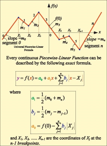
Download figure:
Standard imageFootnotes
- 1
A hysteresis loop is said to be pinched at the origin if it always passes through the origin at all time instants when the input signal waveform is zero. It follows that a pinched hysteresis loop can never intersect the vertical axis except at the origin. For some contrived input signal waveforms, such as figure 3 of [2], or for any periodic signal whose frequency tends to infinity (whereupon the area of the pinched hysteresis loop shrinks to zero) the resulting single-valued function in both cases can be interpreted as the limiting Lissajoux figure of a pinched hysteresis loop because for other periodic waveforms, or for moderate frequencies, a pinched hysteresis would emerge.
- 2
In 1813, Davy was honored and invited to give a lecture and demonstration of his great invention at the London Royal Institute. A picture of Sir Humphry Davy demonstrating his carbon-rod arc discharge lamp is shown in the upper part of figure 1(c). The huge bank of Volta's batteries is shown in the lower part of the picture.
- 3
In spite of a raging war between England and France in 1807, Napoleon Bonaparte was so impressed by Davy's numerous fundamental scientific contributions (including the discovery of the potassium and sodium elements, and the invention of the Carbon arc discharge lamp) that he had decided to award France's most prestigious Prix Napoleon de Institut science prize to Sir Humphry Davy. To bypass the Naval blockade, Napoleon had sent a special courier to sneak into England and deliver to Davy a special diplomatic visa, along with a pouch of gold coins that would cover not only the cost of a luxurious travel between London and Paris for Davy and his wife (lady Jane), but also for a personal servant (who happened to be a young assistant of Davy named Faraday, the inventor of the 'inductor'!) to carry their baggage.
- 4
This simple procedure was proposed by P Georgiou from the Imperial College London [60].
- 5
Each lobe area is found by calculating the corresponding Stieltjes integral [36].
- 6
- 7
The same property can be easily shown to also apply for Extended Memristors.
- 8
Here we mean an 'Ideal' Memristor. For a Generic Memristor, or an Extended Memristor, the preceding section shows that one generally measures a continuously varying dc V-I curve as the dc voltage is tuned over any voltage interval that would not burnt-out the device.
- 9
Sgn(•) is the Signum function: Sgn φ = 1, φ > 0 = −1, φ < 0.
- 10
There is a name for this singular circuit element. It is called a Nullator [44].
- 11
Assuming of course the device behaves like an ideal memristor, or one of its Ideal Generic Memristor siblings.
- 12
- 13
We can easily prove that the limiting Lissajoux figure at high frequencies for an Extended Memristor is not a straight line, but a single-valued curve by modifying the proof on page 212 of [42] for Generic Memristors, where the prediction that the state x(t) must tend to the initial state x0 = x(0) remains valild also for Extended Memristors. See [61] for another example.
- 14
To illustrate that there are many different methods to synthesize and build a locally-active memristor, we opted for a circuit realization which is not derived from the Resistor to Memristor mutator presented in figure 5(b).
- 15
If the pinched point is located near (but not exactly at) the origin, we will call it an imperfect memristor.