

Abstract
The plasma-enhanced chemical vapor (PECVD) co-deposition of pyridine and 1,2 dicarbadodecaborane, 1,2-B10C2H12 (orthocarborane) results in semiconducting boron carbide composite films with a significantly better charge extraction than plasma-enhanced chemical vapor deposited semiconducting boron carbide synthesized from orthocarborane alone. The PECVD pyridine/orthocarborane based semiconducting boron carbide composites, with pyridine/orthocarborane ratios ~3:1 or 9:1 exhibit indirect band gaps of 1.8 eV or 1.6 eV, respectively. These energies are less than the corresponding exciton energies of 2.0 eV–2.1 eV. The capacitance/voltage and current/voltage measurements indicate the hole carrier lifetimes for PECVD pyridine/orthocarborane based semiconducting boron carbide composites (3:1) films of ~350 µs compared to values of ⩽35 µs for the PECVD semiconducting boron carbide films fabricated without pyridine. The hole carrier lifetime values are significantly longer than the initial exciton decay times in the region of ~0.05 ns and 0.27 ns for PECVD semiconducting boron carbide films with and without pyridine, respectively, as suggested by the time-resolved photoluminescence. These data indicate enhanced electron–hole separation and charge carrier lifetimes in PECVD pyridine/orthocarborane based semiconducting boron carbide and are consistent with the results of zero bias neutron voltaic measurements indicating significantly enhanced charge collection efficiency.
Export citation and abstract BibTeX RIS
1. Introduction
Semiconducting boron carbide icosahedral materials have been the subject of extensive investigation for solid state neutron detection [1–13]. Boron-rich icosahedral based semiconductors such as boron carbide [14–18], and other B rich icosahedral solids [14, 19–21] are particularly advantageous in certain situations due to their ability to heal neutron [14] and electron radiation [18, 20] damage. These materials have a number of disadvantages, however, due to limits in current rectification efficiency leading to a constant power drain due to high defect concentrations [22] and low carrier mobilities [23] Although exceptionally high mobilities have been sometimes claimed [24], such claims have not been attributed to plasma-enhanced chemical vapor (PECVD) deposited semiconducting boron carbide.
Echeverria and coworkers [12, 13] recently showed that partially dehydrogenated boron carbide (B10C2Hx where 0 ⩾ x ⩾ 12) combined with aromatic pyridine (C5H5N) linking groups, through the plasma-enhanced chemical vapor (PECVD) co-deposition of pyridine and 1,2 dicarbadodecaborane, i.e. 1,2-B10C2H12 (orthocarborane), provided better current rectification, and displayed significantly better charge collection in zero applied bias neutron voltaic studies. Improved charge collection in a semiconducting boron carbide would significantly improve the utility of this semiconductor as a neutron voltaic [12] and neutron detector in the low neutron flux regime. The increased efficiency would yield a higher sensitivity to the detection of charge pulses associated with 10B fragmentation resultant from a neutron event [1–13, 25].


The improved charge collection, at very low bias for pyridine-containing PECVD films deposited on n-type Si [12, 13] could be due to improved carrier mobilities in this boron carbide and/or because of significant increases in carrier generation and/or carrier lifetimes. Here we explore the latter two issues.
2. Experimental and theoretical methods
2.1. Semiconducting boron carbide film deposition
Film deposition studies were carried out in a system described previously [12, 13, 26]. The deposition of pyridine/orthocarborane composite films was carried out in a custom-built plasma enhanced chemical vapor deposition (PECVD) chamber [12, 13, 26–30], with an inductively-coupled Ar plasma (20 W, 50–70 mTorr total pressure). Films were generally deposited on Ar+ ion cleaned n-doped Si(1 0 0) 1 cm × 1 cm substrates at room temperature, without subsequent annealing. For optical absorption/photoluminescence studies, however, films were deposited on SiO2 substrates. Orthocarborane and pyridine (spectral grade), from commercial sources, were purified by freeze-pump-thaw procedures and introduced into the deposition chamber using mass flow controllers. In the PECVD co-deposited pyridine and orthocarborane semiconducting hydrogenated boron carbide films, the source compounds are partially dehydrogenated, initially by the cation elimination of H2 [31], and thus form a nonvolatile semiconductor [1–13]. While it is more accurate to describe the composite boron carbide films as PECVD co-deposited pyridine and orthocarborane semiconducting hydrogenated boron carbide films deposited on n-type Si, B10C2Hx:Py/Si, such films will be referred to as PECVD pyridine/orthocarborane films with the pyridine to orthocarborane ratios denoted. Those PECVD semiconducting hydrogenated boron carbide films (B10C2Hx/Si), without pyridine, will be denoted in the text that follows as PECVD orthocarborane films.
Composite films with different pyridine/orthocarborane ratios were formed by varying the flow rate of pyridine into the PECVD chamber, with a constant flow rate of orthocarborane at 5 sccm (standard cubic centimeter per minute). Pyridine/orthocarborane ratios were determined by halting the deposition at various times and characterization of the film through x-ray photoemission spectroscopy (XPS), without sample exposure to ambient [12]. The XPS results, in general, did not vary significantly through the deposition process, nonetheless, the stoichiometries reported here represent an average of the results used to determine each film composition. Films with pyridine/orthocarborane ratios of ~2:1, ~3:1, ~5:1 ~7:1, and ~10:1, for example, were obtained with pyridine flow rates of 5 sccm, 7 sccm, 20 sccm, 30 sccm, and 35 sccm, respectively. This procedure provided a high degree of reproducibility of films composition. Film thickness and band gap energies were determined by variable angle spectroscopic ellipsometry (VASE).
2.2. Acquisition and analysis of XPS
Angle-integrated x-ray photoemission spectra (XPS) were acquired using a commercially available 140 mm mean radius hemispherical analyzer with multi-channel plate detector. The XPS spectra were acquired using unmonochromatized Alkα x-ray radiation with a constant analyzer pass energy of 23.5 eV. The XPS spectra were modified for further analysis by Shirley background subtraction [29, 30, 32–34] using commercially available software. Binding energies were charge corrected by setting the Si 2p peak energy level at a binding energy of 99.3 eV [28, 29, 35]. Deconvolution of the B 1s, C 1s and N 1s core level photoemission spectra was accomplished by fitting the core level with a Gaussian–Lorentzian function, with a full width half maximum of 1.5 eV, 1.4 eV and 1.8 eV, respectively, as described previously [12, 28, 29].
As in previous studies [12, 13], the pyridine/orthocarborane ratios of the various films were determined by XPS analysis of the relative B/N atomic ratios by standard methods [33, 34]. This approach of course assumes negligible loss of stoichiometry during decomposition of carborane and pyridine films during the plasma deposition process, an assumption validated by the relative invariance of the B 1s and N 1s spectra for such films in comparison to condensed pyridine or orthocarborane [12, 13, 27–30]. These ratios are displayed in table 1.
Table 1. Experimental B/N and B/C atomic ratios, and corresponding pyridine/orthocarborane ratios with calculated B/N and B/C atomic ratios assuming intact precursors in deposited films.
| Film | Experimental atomic ratio | Pyridine/ orthocarborane ratio | Calculated atomic ratio | ||
|---|---|---|---|---|---|
| B/N | B/C | B/N | B/C | ||
| 1 | 4.76 | 0.75 | ~2:1 | 5.00 | 0.83 |
| 2 | 3.57 | 0.62 | ~3:1 | 3.33 | 0.61 |
| 3 | 1.82 | 0.34 | ~5:1 | 2.00 | 0.34 |
| 4 | 1.43 | 0.26 | ~7:1 | 1.43 | 0.26 |
| 5 | 1.05 | 0.21 | ~10:1 | 1.00 | 0.21 |
Atomic ratios of B/N and B/C were derived from experimental XPS peak intensities. The estimation of the pyridine/orthocarborane ratios and corresponding B/N and B/C atomic ratios were made on the assumption that both the carborane and pyridine moieties remain essentially intact under these plasma deposition conditions, as previously demonstrated [26, 27]. The very good agreement between the experimental and calculated ratios in table 1 also demonstrates that the films contain negligible N or C contamination from extraneous sources.
2.3. Spectroscopic ellipsometry
The variable angle spectroscopic ellipsometry (VASE) measurements were used to determine the film thickness, band gaps and dielectric constant. The ellipsometry data were acquired on multiple instruments, but primarily on a J A Woollam RC2 VASE ellipsometer in ambient conditions. Data were acquired from films deposited on n-Si(1 0 0) substrates, over a range of photon energies in the visible to ultra-violet range (0.73 eV–6.4 eV (1690 nm–193 nm)), in increments of 1 nm (1000 nm–1690 nm) and 2.5 nm (1000 nm–193 nm), respectively. The angles of incidence were varied from 45° to 75°, in 5° increments. Data were fit by standard methods [36–38], using commercially available software. Standard spectroscopic ellipsometry determines the ratio (ρ) of the complex-valued Fresnel reflection coefficients rp and rs and is commonly presented by parameters ψ and Δ where ρ = rp/rs = tan(ψ)eiΔ.
2.4. Optical absorption and emission measurements
Optical characterization of boron carbide films was conducted with UV–Vis spectroscopy and steady-state and time-resolved photoluminescence spectroscopy. Data were acquired from films with a thickness around 1 µm deposited on glass substrate. UV/Vis absorption spectra were recorded with a Jasco V-670 spectrophotometer over a range from 300 to 700 nm. Photoluminescence spectra and photoluminescence decay lifetimes were obtained using an excitation source (Broadband tunable femtosecond Ti:Sapphire laser using second harmonic generation in BBO crystals) at wavelength λ = 400 nm. For photoluminescence decay lifetimes, Hamamatsu R928 photomultiplier tube was used as a photodetector. Photoluminescence decay spectra were extracted from the luminescence 580 nm.
2.5. Capacitive-voltage and current–voltage measurements (Nebraska)
Current–voltage and capacitance-voltage measurements were used to determine carrier (hole) lifetimes in various PECVD co-deposited pyridine and orthocarborane films, deposited on n-type Si substrates with resistivity of 100 Ω · cm. Diode detectors were formed by depositing Ti–Au electrodes, and measurements conducted as described previously [12, 13, 30]. Electrical characterization is comprised of capacitance versus voltage C(V) measurements and current versus voltage I(V) measurements. The C(V) measurements were acquired using an HP Model 4192A Impedance Analyzer with an oscillation voltage set to 0.010 V, at set frequencies increased by decades from 1 kHz to 10 MHz in a 4 point parallel circuit. The I(V) measurements were obtained using a Keithley 2411B SourceMeter to deliver a dc voltage, a Keithley 6485 PicoAmmeter to measure the resulting current, and a HP 3478A multimeter to measure the voltage across the device under load.
2.6. Theoretical methods
First-principles calculations were performed in the framework of density functional theory (DFT), as implemented in the DMol3 code [39, 40]. The PW91 generalized gradient approximation (GGA) was used, in the form of Perdew–Burke–Ernzerhof (PBE) [41], for the exchange-correlation functional because of the better performance of GGA than the local density approximation (LDA) in many molecular systems. All the electrons were considered equally, and the double numerical plus polarization (DNP) basis set, which is comparable to the 6-31G** basis set, was used. The convergence tolerance for the self-consistent field is 2.72 × 10⁻⁶ eV, and the molecular structures were optimized until the maximum force was below 0.054 eV Å−1.
2.7. Band gap determination
The band gaps of PECVD semiconducting pyridine/orthocarborane boron carbide films with pyridine to orthocarborane ratios of ~3:1 and ~9:1, synthesized from PECVD co-deposited pyridine and orthocarborane, were ascertained from variable angle spectroscopic ellipsometry (VASE), and are indicated as vertical arrows in the model dielectric function data shown in figure 1.
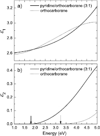
Figure 1. The model dielectric function spectra for PECVD pyridine/orthocarborane and PECVD orthocarborane films: (a) real part of the model dielectric function of a PECVD pyridine/orthorcarborane film (3:1) (solid line) and a PECVD orthocarborane film (dotted line); (b) same as (a) but for the imaginary part of the model dielectric function. Vertical arrows indicate the band gap energy determined using the Tauc–Lorentz model described in the text.
Download figure:
Standard image High-resolution imageA 5 phase optical layer model composed of ambient, surface roughness layer, pyridine/orthocarborane boron carbide film, SiO2 layer, and Si substrate was used to describe the experimental data for spectroscopic parameters ψ and Δ (supplemental data, figure S1 (stacks.iop.org/JPhysD/49/355302/mmedia)) accurately. Literature dielectric function values were used to describe SiO2 and Si and were not further varied during the analysis [42]. The dielectric function of the amorphous pyridine/orthocarborane boron carbide film was described using a Tauc–Lorentz (TL) model [37, 38, 43]:
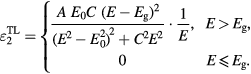
where E0 is the peak transition energy and C is the broadening. The amplitude and band gap energy are denoted by A and Eg, respectively. The Tauc–Lorentz model is combined with a high energy pole and a static offset in order to describe resonant contributions to the dielectric function outside of the investigated spectral range.
Average film thicknesses for PECVD pyridine/orthocarborane films, with pyridine/orthocarborane ratios of 3:1 and 9:1, were determined by this method to be 557(38) nm and 483(22) nm, respectively, in qualitative agreement with the estimates of ~750 nm for both films estimated from extrapolation of XPS-derived growth rates during PECVD (the numbers in parentheses represent VASE-derived thickness non-uniformities for higher accuracy in thickness determination). The PECVD orthocarborane film had corresponding thickness estimates of 980(41) nm from VASE and based on the growth rate, a similar thickness estimate of roughly 1300 nm.
It is well known that the indirect band gap of PECVD semiconducting hydrogenated boron carbide films range from 0.7 eV [37] to 1.7–3.8 eV [44]. Consistent with these prior results for PECVD semiconducting hydrogenated boron carbide films, measurements of several PECVD co-deposited pyridine/orthocarborane films, with 3:1 pyridine to orthocarborane ratios, yielded indirect band gaps of 1.7–1.8 eV. This demonstrates the reproducibility of these films with respect to electronic structure and chemical composition. The best-fit parameters obtained during the analysis of the VASE data for one of these films which is shown in figure 1 are Eg = (1.80 ± 0.01) eV, A = (4.57 ± 0.06) eV, E0 = (5.8 ± 0.1) eV, and C = 2.3 = (4.33 ± 0.04) eV. Slightly smaller band gaps in the region of 1.6 eV were found for PECVD co-deposited pyridine and orthocarborane semiconducting hydrogenated boron carbide films, with a pyridine to orthocarborane ratio of 9:1. These values for the indirect band gap are consistent with our expectations, and indicate that the value of the indirect band gap does not change much over a considerable range of pyridine/orthocarborane stoichiometry. In contrast, the PECVD boron carbide film without pyridine displays indirect band gaps of approximately 3.0 eV. The best-fit parameters obtained during the analysis of the VASE data for one of these PECVD boron carbide film without pyridine which is shown in figure 1 are Eg = (3.2 ± 0.1) eV, A = (4.85 ± 0.06) eV, E0 = (6.5 ± 0.1) eV, and C = (1.50 ± 0.01) eV. This tends to indicate a fairly high degree of hydrogenation in the boron carbide [44] rather than a more boron rich boron carbide [45]. The relationship between absorption coefficient (α) and interband transition probabilities for various types of optical transitions in semiconductors is also related to the direct or forbidden indirect band to band transitions, and this analysis (seen in the supplementary section, yielded similar values for the indirect band gaps, indicating that different approaches to measuring the band gap yield similar values.
The experimental results for band gaps of PECVD pyridine/orthocarborane versus PECVD orthocarborane films are in agreement with trends observed in the DFT calculations. From the calculated orbital binding energies of the highest occupied molecular orbital (HOMO) to lowest unoccupied molecular orbital (LUMO), a modest increase in the number of pyridine linking groups decreases the band gap from 6.6 eV to 2.7 eV, as seen in figure 2, and summarized in figure 3, for the carboranes linked by linear chains of pyridine. Further dehydrogenation and more extensive crosslinking would clearly lead to further decreases in the HOMO-LUMO gap, and this would bring theory more in line with experimental values.
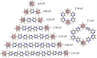
Figure 2. Density functional theory cluster calculations showing a decrease in the band gap, with increasing numbers of linking pyridine moieties. The numbers indicate the highest occupied molecular orbital (HOMO) to lowest unoccupied molecular orbital (LUMO) gap.
Download figure:
Standard image High-resolution image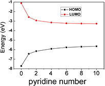
Figure 3. The decrease in band gap from density functional theory (DFT) calculations for an increasing length of the pyridine linear chains linking the closo-carboranes. The band gap tends to 2.08 eV with the increasing number of pyridine moieties, in the linear chain geometry shown above in figure 2.
Download figure:
Standard image High-resolution image4. Exciton formation and lifetime
Absorption spectra acquired for the PECVD pyridine/orthocarborane composite films indicate that the addition of pyridine leads to sharply enhanced absorption at λ > 300 nm (supplemental data, figure S2). This is consistent with the variable angle spectroscopic ellipsometry data for the PECVD pyridine/orthocarborane composite films, indicating a direct band gap in the region of 3 eV (figure 1). Photoluminescence data (with photo-excitation at wavelength = 400 nm) shows that the photoluminescence is centered around 2.06 eV–2.14 eV (wavelength = 600 nm) for PECVD co-deposited pyridine and orthocarborane semiconducting hydrogenated boron carbide films, with 2:1 and 5:1 pyridine to orthocarborane ratios, as seen in figure 4. In general, this indicates an exciton energy that may be larger than the indirect band gap, but smaller than the direct band gap. Since exciton formation is a q = 0 excitation, this implies that in fact there is an indirect band gap. As noted above, however, the highest occupied molecular orbital (HOMO) to lowest unoccupied molecular orbital (LUMO) gap in DFT tends towards 2.08 eV, with the increasing number of pyridine moieties, in the linear chain geometry shown above, and is consistent with the photoluminescence values of 2.06 eV–2.14 eV.
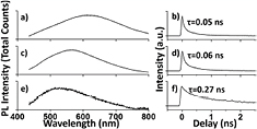
Figure 4. The photoluminescence spectra (left) and corresponding photoluminescence decay data for PECVD pyridine/orthocarborane and PECVD orthocarborane films. (a) photoluminescence spectra for a pyridine/orthocarborane ratio of 5:1 film; (b) corresponding photoluminescence decay (c) and (d) photoluminescence and decay data for a pyridine/orthocarborane 2:1 film; (e) and (f) corresponding photoluminescence and decay data for a PECVD orthocarborane film. Characteristic initial photoluminescence decay times (τ) were obtained from 3-exponential fits to the decay data (b), (d) and (f).
Download figure:
Standard image High-resolution imageIn contrast to the PECVD pyridine/orthocarborane composite films, the photoluminescence data for the PECVD orthocarborane films free of pyridine (figure 4(e)) indicate an exciton (~2.4 eV) smaller than the band gap (~3 eV) could be indicative a more stable exciton than is the case for the PECVD pyridine/orthocarborane composite films (2.6–2.14 eV versus 1.7–1.8 eV respectively) where the exciton energy is larger than the indirect band gap. This increased stability of the exciton in PECVD orthocarborane films is reflected in the luminescence lifetimes.
The decay of the photoluminescence for the PECVD co-deposited pyridine and orthocarborane semiconducting hydrogenated boron carbide composite films (figures 4(b) and (d)) is quite rapid (~0.05–0.06 ns), even faster than the initial decay of photoluminescence for the PECVD orthocarborane films without any pyridine-like moieties (0.27 ns; figure 4(f)). Such indicators of the very rapid decay of the exciton particularly in the PECVD pyridine/orthocarborane composite films, raises the question of how charge extraction from the composite film is possible with any significant current, especially at low bias, as is in fact observed [12, 13]. If exciton unbinding is part of the exciton decay process, and the resulting carriers have appreciable lifetimes, then charge extraction should be more facile than indicated by the very rapid decay of the photoluminescence for the PECVD pyridine/orthocarborane composite films.
From a theoretical perspective, for the closo-carboranes linked by pyridine chains, there is no indication that exciton unbinding is particularly favored in spite of the fact that the cluster calculations show that the spatial placement of the highest occupied molecular orbitals (HOMO) is similar to that of the lowest unoccupied molecular orbitals (LUMO) as seen in figures 5 and 6 respectively. The fact that the LUMO is of orthogonal symmetry to that of the HOMO, suggests a symmetry hindrance to the decay of an electron in the LUMO to a hole at the top of the valence band, if this is applicable to the solid state. Thus a HOMO to LUMO excitation, while spatially overlapping, could well favor an unbinding of the hole and electron states because of the symmetry restrictions, especially when the exciton energy may be larger than the band gap.

Figure 5. The highest occupied molecular orbital (HOMO), as indicated by the yellow and blue colors, of carborane icosahedra connected by a linear chain of linked pyridine moieties.
Download figure:
Standard image High-resolution image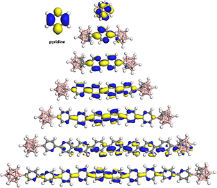
Figure 6. The lowest occupied molecular orbital (LUMO), as indicated by the yellow and blue colors, of carborane icosahedra connected by a linear chain of linked pyridine moieties.
Download figure:
Standard image High-resolution image5. Estimates of the hole carrier lifetimes
The hole carrier lifetimes can be extracted from the diode the current versus voltage I(V) and capacitance C(V) curves using some modest assumptions. Such data is readily obtained given the robust facility for fabrication of successful PECVD semiconducting hydrogenated boron carbide composite films with n-type silicon [3, 4, 9–13]. The I(V) curves for heterojunction diodes containing PECVD pyridine/orthocarborane composite films both with and without the addition of pyridine moieties, i.e. (B10C2Hx:Py/Si; B10C2Hx:/Si), are shown in figure 7.

Figure 7. The current versus voltage curves for the heterojunction diodes PECVD pyridine/orthocarborane composite film on silicon device (pyridine) compared to the PECVD orthocarborane semiconducting hydrogenated boron carbide film on silicon device (undoped).
Download figure:
Standard image High-resolution imageThe series resistance Rs is related to the capacitance [46]:
where  is the angular frequency (
 ),
),  is the frequency of the small signal perturbation across the device under test,
  is the junction capacitance,
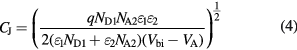
  is the parallel capacitance (measured capacitance in a parallel circuit). Therefore, although the data in figure 7 indicate a higher total resistance for the PECVD orthocarborane boron carbide film diodes without pyridine, the lower Rs of the PECVD pyridine/orthocarborane composite film on silicon diode is evident in figure 7 from the more pronounced exponential form, following the ideal diode equation [47]:
where  is the saturation current,
  is the elemental charge,
  is the applied voltage,
  is the Boltzmann constant, and
  is the temperature. The PECVD pyridine/orthocarborane composite film sample also does not exhibit signs of breakdown within the measured voltage range.
By definition, the low frequency conductance

is the slope of the I(V) curve at the d.c. operating point (i.e. f → 0 Hz) The low frequency conductance (G0) is dependent on the carrier lifetimes, depletion width of the diode junction, built in voltage, doping profile, and carrier concentration. It should be emphasized however, that regardless of the junction type or dominant current component, G0 = dI/dVA can always be applied to the measured I(V) data in order to determine G0 [47], and that has been done in this instance. The purpose of the examination of G0 becomes immediately apparent in the analysis of the capacitance data.
The low frequency conductance (G0) of both diodes has been plotted in figure 8. It is immediately evident that the measurement for the PECVD orthocarborane film, without pyridine, is much more noisy than the PECVD pyridine/orthocarborane composite film on silicon device. There is also a much greater initial increase in the current for equivalent applied voltages in the PECVD orthocarborane film (pyridine-free) on silicon diode. Near 2.5 applied volts, however, the change in current with increasing voltage flattens, and becomes linear for the PECVD orthocarborane film (pyridine-free) on silicon diode. A linear  is what one would expect from a resistor. In contrast, the PECVD pyridine/orthocarborane composite film on silicon diode exhibits an exponential increase in current when responding to increased applied voltage. This is expected since the derivative of an exponential function (2) is still an exponential function.
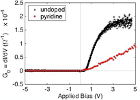
Figure 8. Low frequency conductance of the PECVD pyridine/orthocarborane composite film on silicon device (pyridine) and PECVD orthocarborane semiconducting hydrogenated boron carbide film on silicon device (undoped) heterojunctions calculated from the I(V) data of figure 7.
Download figure:
Standard image High-resolution imageThe capacitance associated with oscillations in the depletion width due to small sinusoidal perturbations is referred to as the junction capacitance ( ). If there are no other charge oscillations, the device capacitance, independent of frequency, is equal to
  in reverse bias (depletion conditions) [48].
where  is the elemental charge,
  is the number of donor atoms/cm3 in the n-type material,
  is the number of acceptor atoms/cm3 in the p-type material,
  is the dielectric constant of the n-type material,
  is the dielectric constant of the p-type material,
  is the built in voltage due to both materials (
 ), and
  is the applied voltage.
Since the junction capacitance is associated with reverse bias conditions, the minority carrier concentration near the edge of the depletion region is very small compared to that of the majority carriers, and thus can be neglected. Under forward bias conditions, this is not a valid assumption. There is a significant contribution by the minority carriers to the changes in charge due to the sinusoidal perturbation signal. This contribution to the device capacitance is referred to as the diode diffusion capacitance ( ), and is given by the equation:
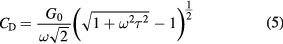
where  is the low frequency conductance previously defined and shown in figure 5,
  is again the angular frequency
  , and
, and  is the effective carrier lifetime. There are many and various contributions to the capacitances, and many types of defects, but if we restrict our modeling efforts to the diffusion component of transport, equation (5) can be used to model the data relative to the baseline capacitance as in figure 9. The C(V) curves of the PECVD orthocarborane boron carbide film, without pyridine, in a heterojunction diode on n-type silicon (i.e. B10C2Hx/Si) (a) and PECVD pyridine/orthocarborane composite films on n-type silicon (B10C2Hx:Py/Si) (b), are compared in figure 9. The first distinction between the PECVD semiconducting hydrogenated boron carbide without pyridine (B10C2Hx/Si) and PECVD semiconducting hydrogenated boron carbide composite films with pyridine moieties (B10C2Hx:Py/Si) is the difference in the reverse bias capacitance values. If the measured capacitance (
 ) →
) →  as discussed above, there should not be a frequency dependent component. The PECVD pyridine/orthocarborane composite film on n-type silicon, B10C2Hx:Py/Si, heterojunction diode exhibits this behavior, but the data for B10C2Hx/Si diode does have a frequency-dependent component to it, meaning that there is another capacitive component present in reverse bias other than
  . This could be an interfacial capacitance, or related to the defect density distribution of the film. The capacitance does decrease with increasing frequency, however, indicating that there is some type of charge carrier that can no longer respond to the perturbation signal as the frequency increases [49–51].
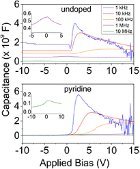
Figure 9. The capacitance versus voltage curves of the (a) the PECVD orthocarborane boron carbide films, without pyridine, on silicon (B10C2Hx/Si) and (b) the PECVD co-deposited pyridine and orthocarborane boron carbide films on silicon, B10C2Hx:Py/Si, as a function of frequency, are compared. The insets are of high frequency data on an expanded capacitance scale.
Download figure:
Standard image High-resolution imageThe peak capacitance values of the PECVD co-deposited pyridine and orthocarborane boron carbide films on silicon, B10C2Hx:Py/Si, diodes are slightly larger than those of the PECVD orthocarborane boron carbide films on silicon, B10C2Hx/Si, heterojunction diodes. There is also a shift of the peak capacitance toward positive bias in the PECVD co-deposited pyridine and orthocarborane boron carbide films on silicon, B10C2Hx:Py/Si, diodes, which is attributed to a decrease in the Rs of the pyridine containing PECVD co-deposited pyridine and orthocarborane boron carbide films on silicon. With the higher Rs, exhibited by the pyridine-free PECVD orthocarborane boron carbide film, there is an associated voltage drop across the junction, which will reduce the applied voltage,

(where  is the junction voltage,
  is the applied voltage,
  is the current, and
  is the series resistance) shifting the signal toward zero, as observed.
There is a change in the capacitance as a function of frequency for all of the PECVD boron carbide films on silicon. This resembles observations from Kaya et al [52] in the high frequency perturbations which were attributed to Rs in the positive applied bias region above the built in voltage range. For the upward curve in the small forward bias, accumulation region, this is well described by the diffusion capacitance CD equation(5).
The modeled  values have been fitted onto the measured C(V) data for 10 kHz, and the agreement between our model and the data is very good for both diodes, as seen in figure 10. The carrier lifetime value varies the height and slope of the small forward bias rise in the C(V) curve. From equation (5) we see that the diffusion capacitance is only a function of G0, ω = 2πf and carrier lifetime (
 ).
).  is taken directly from I(V) measurement, f the driving frequency, set during the measurement was set during the C(V) measurement. This leaves only carrier lifetime as the variable to adjust the diffusion capacitance value. Curve fitting equation (5) to the measured C(V) data in figure 9, taken at 10 kHz for both diodes yields a best fit of the measured data, for the carrier lifetime was found to be 350 µs in the PECVD pyridine/orthocarborane boron carbide films on silicon, B10C2Hx:Py/Si, heterojunction diode, and 35 µs in the PECVD orthocarborane boron carbide film on silicon, B10C2Hx/Si, heterojunction diode.
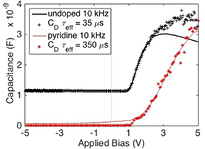
Figure 10. Model of diffusion capacitance overlaid on C(V) data at 10 kHz: undoped data (solid black line) and pyridine doped data (solid red line). The undoped calculated  (black +) indicates an effective carrier lifetime of 35 µs. The pyridine doped calculated
  (red *) indicates an effective carrier lifetime of 350 µs.
Download figure:
Standard image High-resolution imageAs noted above, the PECVD pyridine/orthocarborane boron carbide films on silicon, B10C2Hx:Py/Si, heterojunction diode has only has 1 frequency dependent capacitance component, the diffusion capacitance. The PECVD orthocarborane boron carbide film on silicon, B10C2Hx/Si, heterojunction diode has two distinct frequency dependent capacitance components. The first is the diffusion capacitance, common to both types of heterojunction diode. The second component, however, indicates that the PECVD boron carbide films, without pyridine, also have defect states that respond to the small signal perturbation, consistent with the large Urbach tail discussed in the supplementary materials and elsewhere [44]. As the period of the perturbation approaches the lifetime of the carriers due to the defect state, the defects can no longer respond to the perturbation, and no longer contribute to the capacitance of the diode. Traps result in contributions to capacitor charging current, but since their time constants are relatively long, the effects of the traps are absent, or greatly reduced, with high frequency perturbations.
If there is a distribution of trap states inside of the band gap of the PECVD orthocarborane film, without pyridine moieties, as the perturbation frequency is increased, there should be a corresponding decrease in the device capacitance. This is exactly what is observed in figure 9 and explains the leaky nature of the I(V) curve of figure 7, for the PECVD orthocarborane boron carbide films (without pyridine) on silicon, B10C2Hx/Si, heterojunction diode. This indicates that that the addition of pyridine to the PECVD semiconducting hydrogenated boron carbide is eliminating key trap states within the device.
Further evidence for this hypothesis is found in figure 10, with the increase in the effective carrier lifetime from 35 µs for the PECVD orthocarborane boron carbide film on silicon, B10C2Hx/Si, heterojunction diode to 350 µs for the PECVD pyridine/orthocarborane boron carbide films on silicon, B10C2Hx:Py/Si, heterojunction diode. One might expect that with the addition of pyridine-like moieties, there would be additional scattering centers, leading to a shorter lifetime. Just the opposite is observed. One possible explanation is the reduction in the trap concentration, as put forth above. A 350 µs carrier lifetime is similar to that reported in diamond like carbon (DLC) films (0.3 ms surface, 0.11 ms bulk) [53], and much longer than the carrier lifetimes for a-Si:H films (~0.1 µs) [54]. Our hole lifetimes for the PECVD pyridine/orthocarborane boron carbide films, however, are in rough agreement with the findings of Bao et al [55] for sputter-deposited boron carbide films quite different for those reported here, indicating carrier lifetimes of 0.91–0.98 ms. A likely distinction between the Bao et al boron carbide films [55] and the films of this study is the presence of hydrogen in the PECVD boron carbide films.
What is key is that the PECVD pyridine/orthocarborane boron carbide films exhibit much longer carrier lifetimes than PECVD orthocarborane boron carbide films without pyridine. This is hugely consistent with the better charge extraction seen upon neutron capture as seen in figure 11.

Figure 11. Experimental neutron pulse height spectra of heterojunction PECVD co-deposited pyridine and orthocarborane boron carbide composite films on n-type silicon are shown in figure 8, for the semiconducting hydrogenated boron carbide with (+++++) B10C2Hx:Py ratio approximately 1:10 and without(•••••) pyridine, i.e. B10C2Hx. Both pulse height spectra were obtained at 0 V Bias. Adapted from [12].
Download figure:
Standard image High-resolution image
The neutron voltaic pulse height spectra at zero bias for a PECVD pyridine/orthocarborane boron carbide on silicon, B10C2Hx:Py/Si, heterojunction diode (10:1 pyridine/orthocarborane) and a PECVD orthocarborane boron carbide on silicon, B10C2Hx/Si, heterojunction diode are compared in figure 11. As expected, the devices exhibit distinctly different spectra. The pyridine-containing PECVD pyridine/orthocarborane boron carbide on silicon heterojunction diode presents a clearly separated peak, representative of much larger pulse height and of significantly higher intensity compared to the pure boron carbide, as reported previously [12]. This signature in the pulse height spectra clearly indicates the improved electron–hole separation, and better charge collection of the electron–hole pairs generated after neutron capture for the PECVD pyridine/orthocarborane boron carbide film than is expected for a PECVD hydrogenated boron carbide on silicon heterojunction device, under low or zero bias conditions [10, 12]. Incomplete charge collection of 10B neutron capture generated electron–hole pair production is expected for solid state devices, especially for very thin films at zero bias [10]. For very thin films of the boron containing semiconductor, the behavior seen here is similar to that observed at higher reverse bias [10] for thin boron containing solid state neutron detectors.
6. Summary
The data presented here demonstrated that PECVD films of co-deposited pyridine and orthocarborane boron carbides exhibit significantly enhanced electron–hole separation, and an order-of-magnitude enhancement of carrier lifetime relative to similar films without pyridine. The pyridine-containing PECVD pyridine/orthocarborane boron carbide films also exhibit carrier lifetimes (figure 10) that are an order of magnitude larger (350 µs) than for the PECVD orthocarborane boron carbide films without pyridine.
The findings of substantially enhanced electron–hole separation and carrier lifetime in PECVD pyridine/orthocarborane boron carbide films versus PECVD orthocarborane boron carbide films without pyridine are certainly encouraging for the application of these materials as solid state neutron detectors. We have shown that the addition of pyridine linking groups to PECVD semiconducting hydrogenated boron carbide films, synthesized on n-type silicon, increases the charge collection, after neutron capture, in a heterojunction diode with silicon at zero bias, and the charge collection is much improved compared to heterojunction diodes fabricated by PECVD but without pyridine. The spatial overlap of the HOMO and LUMO states in cluster calculations, if applicable to the solid, suggests that exciton decay is facile, but hindered by symmetry constraints.
Acknowledgments
This work was supported by the Defense Threat Reduction Agency (Grant No. HDTRA1-14-1-0041), the National Aeronautics and Space Administration through grant 13-EPSCoR-0012 and the National Science Foundation through the Nebraska Materials Research Science and Engineering Center (Grant No. DMR-1420645). The authors would like to thank Shireen Adenwalla for technical assistance and discussion. ERW was supported by Nebraska Public Power District through the Nebraska Center for Energy Sciences Research and an SRC research fellowship associated with C-SPIN, part of STARnet, a Semiconductor Research Corporation program sponsored by MARCO and DARPA (SRC 2381.002 and 2381.003). GP was supported by the Office of Research and Economic Development at the University of Nebraska-Lincoln.