

Abstract
Hybrid photovoltaic cells take the advantages of silicon in charge carrier separation and transport and organic dyes in strong complementary light absorption. Photovoltaic responses from a set of hybrid solar cells based on amorphous silicon and phthalocyanine dyes of double- or triple-layer heterojunction structures were investigated, which were found to have thickness dependence with the organic active layers. It was found that the photocurrent contributions from organic layers are limited, although they are strong light absorbers. The main photocurrent contributions are from the silicon counterpart.
Export citation and abstract BibTeX RIS
1. Introduction
The development of alternative forms of energy has been of global interest in recent years. An overflowing solar energy is a particularly promising clean and readily available source for future sustainable production of fuel and electricity. Solar cells made from silicon or inorganic compound semiconductors have met the basic application requirements [1, 2]. Crystalline silicon cells have been widely manufactured and have occupied over 90% of the world total photovoltaic (PV) cell production [3]. However, crystalline silicon technology is still too expensive to manufacture. Amorphous silicon thin film and organic solar cells are low-cost alternatives particularly suitable in flexible, light-weight and arbitrarily-shaped devices, which may promote potential applications in a wide field of industries.
Flexible and portable energy devices have attracted tremendous attention in recent years, such as fibre solar cells [4–7], battery [8], integrated power fibre [9–11], super-capacitors [12–14] and solar cells on textiles [15, 16]. The advantage of these flexible devices is the possibility of incorporating them in wearable technology. Due to traditionally inorganic crystalline semiconductor cells such as silicon being rigid, they are inherently not compatible with textiles where flexibility is required. Although inorganic thin film solar cells fabricated on metal wires [17], metal foils [18] or polymer substrates [19] were reported, problems like moving interconnects, shadowing, mechanical resilience, mismatch in thermal expansion coefficients of the polymer foils and inorganic solar cell materials, and durability need to be conquered [15]. Meanwhile, organic and dye-sensitized solar cells combined with fabrics have been extensively studied, but preventing moisture and oxygen permeation into the sensitive organic or dye materials remain a challenge [20–24]. Many inorganic materials are advantageous because of their higher thermal and/or chemical stability than their organic counterparts. They have relatively large dielectric constants which are advantageous in charge dissociation and relatively high carrier mobility. It is anticipated that the hybrid structures may combine the flexibility and the strong complementary absorption of organic materials with those of inorganic materials to achieve high power conversion efficiency (PCE).
The fabrication of amorphous silicon (α-Si : H) thin film involves low-cost plasma-enhanced chemical vapour deposition (PECVD) technology. In addition to α-Si : H being more flexible than crystalline Si, it absorbs more strongly in the optical spectral range. It is therefore the preferred choice in hybrid device fabrication [25]. The accepted best PCE for an amorphous silicon p–i–n cell has been about 10% since 2009 [2]. As far as organic materials are concerned, macromolecules are generally more stable than their low-molecular-weight counterpart and withstand harsh conditions in amorphous silicon fabrication. A few organic polymers have been investigated to use in a hybrid device with α-Si : H layers. Gowrishankar et al [25] proposed that under illumination excitons in the hybrid structure of α-Si : H and organic polymers could be separated and collected by either of two mechanisms, i.e. exciton diffusion to the polymer-inorganic interface followed by forward electron transfer from the polymer to the inorganic semiconductor and Förster-like energy transfer prior to hole transfer from the inorganic back to the polymer. In both mechanisms, the final state is an electron in the inorganic semiconductor and a hole in the polymer and these carriers are collected at the electrodes. A recent report worked on poly(3-hexylthiopene) (P3HT) or P3HT : [6,6]-phenyl-C61-butyric acid methyl ester (PCBM) on top of α-Si : H and found that the efficiencies were similarly low [26]. Our previous investigation demonstrated that in α-Si : H/polymer hybrid solar cells, device performance depended strongly on the dopant types (intrinsic, n-type or p-type α-Si : H), with an intrinsic Si hybrid device performing the best and speculated existing unbalanced charge transport [27]. This was soon confirmed via experiments that balancing the hole mobility in the polymer and the electron mobility in amorphous silicon was critical in improving PV performance of the hybrid devices [28]. An exciting PCE value of 4.7% was achieved. This is very encouraging.
Although there has been much investigation, mechanisms associated with the hybrid interfaces at the organic and inorganic junctions are not fully understood. Small molecules can be better defined so they can be more suitable to use in order to reveal the physical mechanisms of the organic–inorganic hybrid junction without the complication of polymers. In contrast to other inorganic semiconductors, hybrid PV devices of silicon (films or substrates) with organic dyes have been the least investigated, although silicon solar cell technology is rather mature. Up to now, there has been only limited literature on thermally-deposited organic small molecules on a crystalline silicon wafer to fabricate a PV device [29–33] and extremely few reports on an α-Si : H or µc-Si thin film [34].
Early hybrid cells of organic/silicon were prepared, such as PbTe(n-type)/CuPc/HF-treated Si(1 0 0)(p-type wafer) with PCE = 3.46% [29] and a-Si : H (p–i–n)/tetra-(4-pyrydil)-porphine with PCE = 3.22% [32], which were almost inorganic devices and the organics were there only to improve light absorption. Organic/Si hybrid conjunction cells of quaterthiophene/HF-etched Si(1 0 0) (n-type wafer) [31] and CuPc/n-type nanoporous Si[33], with PCE were about 0.9 and 2%, respectively. Hybrid cells with MgPc/etched Si(1 0 0) wafer (n-type) [30] and MgPc/etched Si(1 0 0) wafer (p-type)[33] heterojunctions were fabricated, which demonstrated PCEs of 0.01–1% depending on the thickness of the organic layer and 2.71% depending on the incident light power, respectively.
Preliminary work on hybrid junctions obtained with simultaneous or sequential deposition of FxZnPc during the remote hot-wire chemical vapour deposition (HWCVD) of µc-Si film gave bulk composite and p–i–n hybrid structures[34]. However, the device efficiencies were not reported. In a more recent report, Chao fabricated a hybrid device with a p–i–n hybrid structure of pentacene (n-type)/a-Si : H (intrinsic)/a-Si : H (p-type) using PECVD for the Si layer and achieved PCE = 3%, where in the preparation pentacene was deposited on top of the a-Si : H film [34]. Pentacene is commonly known to be a p-type material in organic devices in conjunction with n-type organics, e.g. fullerene and perylene derivatives. To use pentacene as an n-type material in a hybrid device is quite unusual. Although the hybrid cells made of silicon wafer and organic interface seems to work fine, the successful cases of hybrid devices made with amorphous silicon and organic interface were extremely few. The physical mechanisms of the devices and interface problems of hybrid structures remain unsolved. A proper understanding of the devices may help to overcome the shortcomings of each when used individually and may improve device performance of hybrid structures.
Phthalocyanines (Pcs) are a class of disc-like or so-called graphene-like organic molecules with attractive photoactive properties, such as relatively high carrier mobility compared to other organics and the potential of having the comparable magnitude carrier mobility of graphite [35–37] as well as excellent chemical stability which can withstand HWCVD fabrication up to 300 °C[34]. Metal Pc (MPc), such as copper Pc (CuPc) and zinc Pc (ZnPc) derivatives are generally and widely used as p-type semiconductors in organic PV cells [38–41]. The optical and transport gaps of Pcs (CuPc and H2Pc) were found to have suitable values [42]. In addition, MPcs are photo-sensitizing with absorptions extending throughout ultra-violet, visible and near IR spectral region, which is complementary to that of amorphous silicon. Therefore, they become ideal candidates to be selected as an organic layer with amorphous silicon in hybrid-device fabrication.
In this work, a simple set of hybrid structures, α-Si : H (intrinsic)/MPc bilayers and multi-layer PV devices were fabricated. Their PV performances were measured and analyzed in order to understand the physical mechanisms in photocurrent generation across amorphous silicon/dye interfaces.
2. Experimental
Hybrid thin-film devices were deposited on indium–tin oxide (ITO) glass substrates with a surface resistance 10 Ohm sq−1 (CSG Holding co., China). The ITO substrates were previously etched into patterned electrodes and cleaned with ethanol, acetone and isopropanol in three successive steps of 15 min each in an ultrasonic bath, and were then dried under nitrogen flow. Pc layers were thermally evaporated under high vacuum of 5 × 10⁻⁶ Torr onto the ITO substrates at a growth rate of 0.03–0.06 nm s−1, monitored by an oscillating quartz thickness controller. Intrinsic amorphous silicon (a-Si : H) was deposited on organic dye layers by a low-power RF excited PECVD (RF-PECVD) from SiH4 at a flow rate of 10 sccm under pressure of 0.5 mbar and using 30 W of RF power at 13.56 MHz applied to two 150 mm diameter parallel plate electrodes. The substrates were placed on the lower electrode which was heated to 200 °C. The a-Si : H film prepared was characterized similarly to previous work [27, 28]. Finally, aluminium was deposited as a top electrode of the device through vacuum evaporation. A shadow mask was used in Al deposition to define active areas that were about 0.03 cm2 in size, with six device-active areas per slide and several samples tested for each device type for reproducibility, as depicted in [43]. The thickness of a-Si : H films in these devices was 200 nm. The thicknesses of the silicon layers were determined by a stylus profilometer (Dektak) and that of Pc films by a surface profiler (Ambios Technology XP-2). Double-layered devices ITO/MPc/a-Si : H/Al and triple-layered device: ITO/CuPc/ZnPc/a-Si : H/Al were finally obtained for investigation. These films were deposited on quartz slides in parallel for optical absorption measurement.
Optical absorption spectra of the materials were recorded using a UV-Vis absorption spectrometer (Shimadzu UV-3101PC). Dark and illuminated I–V characteristics of the devices were measured with a Keithley 2440C source meter using a computer controlled program. A solar simulator was used as a light source. Photocurrent spectra were measured using a Bentham spectrometer. All measurements described above were carried out at ambient conditions.
3. Results and discussion
MPcs are a class of highly stable organic material, neither soluble in common organic solvent nor fusible up to 400 °C when they begin to decompose [44]. They are expected to be stable enough at 200 °C in plasma bombardment. Because there is no PV response for intrinsic α-Si : H only or Pc only devices, double-layered hybrid devices using organic CuPc and a-Si : H have been prepared. The devices have a configuration of ITO/CuPc/a-Si : H/Al, with thicknesses of the organic layers varying in a range of 30–130 nm.
Current–voltage characteristics of the CuPc/a-Si : H devices both in the dark and under illumination (as shown in figure 1) were measured. The dark I–V curves showed general rectifier behaviour. PV responses under illumination were detected and the device parameters were extracted, i.e. open-circuit voltage (VOC), short-circuit current (ISC), and fill factor (FF) as listed in table 1.
Table 1. Characteristics of PV devices with a structure of ITO/organic layer/a-Si : H /Al under illumination at 100 mW cm−2, where the EQE is the peak value measured at the wavelength as indicated.
| Devices (organic layer thickness) |  (V) (V) |
 (mA cm−2) (mA cm−2) |
FF (%) | EQE (%) |
RS (Ω) | RSH (Ω) |
|---|---|---|---|---|---|---|
| CuPc layer | ||||||
| 30 nm | 0.09 | 0.33 | 28 | 3.4 (385) | 4.8 × 10² | 1.4 × 10³ |
| 50 nm | 0.16 | 0.51 | 26 | 5.0 (400) | 8.5 × 10² | 1.7 × 10³ |
| 70 nm | 0.30 | 0.48 | 26 | 7.7 (405) | 1.0 × 10³ | 1.9 × 10³ |
| 90 nm | 0.38 | 0.39 | 32 | 8.7 (405) | 7.2 × 10² | 4.4 × 10³ |
| 110 nm | 0.46 | 0.75 | 30 | 4.4 (405) | 7.9 × 10² | 2.1 × 10³ |
| 130 nm | 0.48 | 0.84 | 30 | 3.8 (405) | 8.6 × 10² | 2.3 × 10³ |
| ZnPc layer | ||||||
|---|---|---|---|---|---|---|
| 30 nm | 0.29 | 1.44 | 27 | 8.2 (400) | 4.1 × 10² | 6.3 × 10² |
| 70 nm | 0.34 | 1.47 | 31 | 8.4 (415) | 2.9 × 10² | 8.7 × 10² |
| 110 nm | 0.52 | 1.47 | 29 | 3.2 (405) | 6.1 × 10² | 1.5 × 10³ |
| CuPc/ZnPc layer | ||||||
|---|---|---|---|---|---|---|
| 40 nm/40 nm | 0.39 | 0.96 | 30 | 5.5 (405) | 5.8 × 10² | 1.6 × 10³ |
aErrors of measurements are about ±0.01 V. bErrors of measurements are about ±0.02 mA cm−2. cErrors of measurements are about ±0.2%.
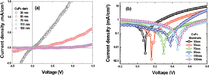
Figure 1. Current–voltage characteristics of ITO/CuPc/α-Si : H/Al devices in the dark (a) and under illumination (b).
Download figure:
Standard image High-resolution imageIt was found that these parameters are closely related to the thickness of the CuPc layers. Both VOC and ISC appeared to increase steadily as the thicknesses of the CuPc layers were increased. FFs of the devices were in a similar range. Shunt resistance (RSH) and series resistance (RS) of these devices can be estimated from slopes of I–V curves around short-circuit current and open-circuit voltage. It was found that RS or RSH between different device structures were of the same magnitude. (table 1) A trend that the RSH rose very slightly can be observed as the organic layer thickness increased. The similarity in RSH demonstrated the degree of lost charges due to recombination and trapping remains at a similar level, which relates to the bulk conductivities [45, 46]. Device performance improved only slightly with an increase in RSH. Since RS reflects the formation of a space-charge accumulation at the interface which appears in opposition to the current flow [45], the above result means that the devices have very similar interface properties.
In order to determine the photocurrent contribution from each layer inside the devices, photocurrent response spectra or external quantum efficiency (EQE) spectra of the hybrid double-layered devices have to be measured, which can be compared with optical absorption spectra of CuPc, α-Si : H and the hybrid films. Figure 2(a) shows the absorption spectra (normalized) of α-Si : H and CuPc thin films. The Pc derivatives have two strong absorption peaks, a high-energy B-band at 335 nm and a low-energy Q-band starting from about 600 nm and extending further into near infrared region [44]. The EQE increased and then decreased against the increasing thickness of CuPc and reached its maximum at wavelength around 405 nm as shown in figure 2(b). The reason might be that as the CuPc film thickness increased, shunt resistance and device performance both improved to a point, but then the device performance will be limited primarily by series resistance which relates to the transport efficiency and collection efficiency of the charge carriers responsible for electron–hole separation at the organic–inorganic interface. It was found that the photocurrent in the hybrid cells showed no response at short-wavelength region at all, which fell in the strong absorption region from the organic CuPc layer at ~335 nm and also from the a-Si : H layer. The photocurrent in the hybrid cells responded well in blue spectral range, but it was mainly contributed from a-Si : H layer. At a longer wavelength region, where organic CuPc layer absorbed strongly above 600 nm, only a small photocurrent response was observed. (see figure 2(b)) The result demonstrated that although the organic CuPc layer was placed at the top of the devices, the light absorption in the organic layer seems not to contribute much to the photocurrent, which is probably caused by insufficient charge carrier separation and transport. When the thickness of Pc is pretty thin (30–50 nm), the optical absorption of Pc is too weak and hardly contributes to the EQE. As the thickness increases, Pc does contribute to the photocurrent with a slight rise at the long wavelength, although it is not the major part with a slight shift in the EQE spectra. This explains a relatively low short-circuit current. The a-Si : H layer played the key role and contributed mainly to the photocurrent.
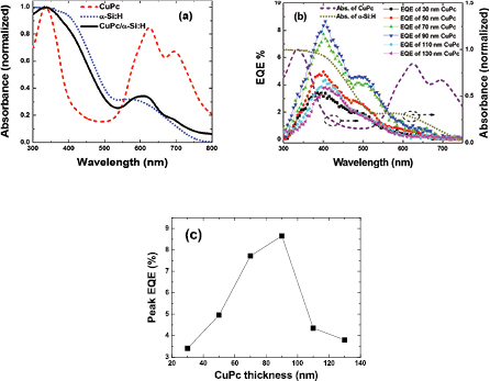
Figure 2. (a) Optical absorption spectra and (b) Photocurrent response spectra of ITO/CuPc/α-Si : H/Al devices. (c) Peak photocurrent response spectral dependence on the CuPc thickness.
Download figure:
Standard image High-resolution imageDouble-layered hybrid ZnPc/α-Si : H devices were fabricated to replace the CuPc, with thicknesses of the ZnPc layers of 30, 70 and 110 nm. Their current–voltage and PV characteristics were measured (see figure 3 and table 1). The VOC variations were very similar to those of the CuPc/a-Si : H devices which increased as the thickness of the ZnPc layer increased. However, the JSC of the ZnPc/α-Si : H devices appeared to remain constant. FFs were within the same range. Photocurrent response spectra of ZnPc/α-Si : H bilayer junction devices (figure 4) appeared rather similar to those from CuPc/a-Si : H devices, with an EQE maximum located at 405 nm for all devices indicating that the main contribution to the photocurrents comes from the a-Si : H layer and a limited contribution from the ZnPc layer.
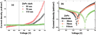
Figure 3. Current density–voltage characteristics of ITO/ZnPc/a-Si : H/Al devices in the dark (a) and under illumination (b).
Download figure:
Standard image High-resolution image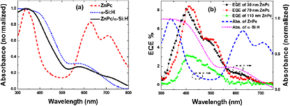
Figure 4. Optical absorption spectra (a) and photocurrent response spectra (b) of ITO/ZnPc/a-Si : H/Al devices.
Download figure:
Standard image High-resolution imageIn order to understand the hybrid device performance and problems within, functionalities of the organic layers in the hybrid devices can be analysed. It is clearly seen from table 1 that the devices incorporating a ZnPc layer performed generally better than the devices with a CuPc layer. The short-circuit current JSC of the ZnPc/a-Si : H devices is much improved over that of CuPc/a-Si : H devices of the same thickness. Consequently, ZnPc/a-Si : H cells give rise to slightly better performance than those of CuPc devices.
Further investigation was carried out by manipulating the active layer using two Pc dyes to fabricate an organic double layer, i.e. a heterojunction CuPc/ZnPc bilayer structure. The organic bilayer structure replaced the single Pc layer and the devices had a configuration of ITO/CuPc (40 nm)/ZnPc (40 nm)/a-Si : H (200 nm)/Al. Current–voltage characteristics and photocurrent spectra are shown in figure 5. It can be seen from the EQE spectra that the multilayer CuPc/ZnPc improves neither the photocurrent output nor other PV parameters of the device, although the additional Pc layer offered better light absorption. The photocurrent contribution of the multilayer device was from the a-Si : H layer.
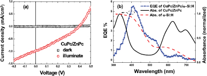
Figure 5. (a) Current density–voltage characteristics and (b) photocurrent response spectra of ITO/CuPc/ZnPc/a-Si : H/Al devices under illumination.
Download figure:
Standard image High-resolution imageThe JSC of the organic devices may be determined by a number of factors: absorption coefficient of the organic layers, the effective area of the donor–acceptor junction, the absorbed light intensity distribution inside the cell, the diffusion and dissociation efficiency of the excitons, the transport efficiency of the charge carriers, and the collection efficiency of the charge carriers.
Electronic properties of Pc derivatives as semiconductors have been investigated most intensively for decades. Pc derivatives are frequently reported being used as a buffer layer in order to enhance the charge transportation capability of the devices by improving contacts or reducing contact resistance at electrodes of the organic semiconducting devices [47, 48]. Recently, Terao et al [49] reported a number of Pcs in heterojunction solar cells with fullerene. According to their results, the differences in p–n junction width or absorbed light intensity distribution in CuPc and ZnPc related devices are negligible. The collection efficiency of holes at the interfaces between the CuPc or ZnPc and the anode could be assumed to be the same. They found that the exciton diffusion lengths of CuPc and ZnPc were similar (15.4 nm for CuPc; 15 nm for ZnPc) although this was slightly different to other reports in the literature, i.e. 10 ± 3 nm for CuPc [50] and 30 ± 10 nm for ZnPc [51, 52]. Both CuPc and ZnPc are recognized as p-type semiconductors, and their hole mobilities (μh) obtained by the space-charge-limited current (SCLC) method [53, 54] or the field-effect transistor (FET) method [55] are similar, which is normally one order of magnitude lower than that of the amorphous silicon (~10–1 cm2 V−1 s−1). From our previous work with polymer/a-Si : H devices, it was found that a compatible hole and electrode mobility was a key factor to improve the hybrid device performance. A relatively efficient hybrid device can be obtained from a hybrid polymer/a-Si : H structure with one magnitude difference in hole/electron mobility [28]. However, it appeared not to be the case in the current work. A different mechanism may be responsible.
In order to understand the device function, reverse currents of the devices were further compared (not shown). It was found that the current continues to increase with reverse bias voltage in all devices which probably indicates a field-dependent carrier collection that is not satisfied by the junction built-in field (too weak or too narrow), rather than indicating a shunt path across the junction. An increase in organic film thickness appears to improve shunt resistance and hence the device performance to a point, then the device performance will be limited by the raising of the series resistance from the devices. Hence, there is a limit to the thickness that can be increased.
Although this work has kept the device structure simple and easy to understand, it should be said that a simple device structure without a buffer layer may face a common problem in contact. It can be particularly obvious if a relatively low transport material was used, which may result in a relatively high series resistance and limited photocurrent reaching the collection electrodes. In turn, it may reduce the FF since the latter is a parameter that is very sensitive to the device construction, in addition to the bulk-material properties, thickness of the active organic layer, degradation and the physio-chemical morphology of the electrode-active layer interface [56]. These can be solved in future device optimization to improve the contact at the interfaces.
The absorption and photocurrent spectra were further analysed in order to find other possibilities responsible for the relatively low JSC of the devices. Although MPc and α-Si : H have a complementary absorption, it is interesting to see that the devices have a good blue response which is normally poor in silicon cells due to a top 'dead layer' . After comparing the absorption from both Pcs and a-Si : H, it can be found that photocurrents in these devices are mostly from absorption in a-Si : H, similar to that reported in the literature [57]. In our devices, almost no short wavelength response can be seen from the (top) organic layer's absorption at ~330 nm, but a small photocurrent contribution is evident from the start (~500–550 nm) of the longer wavelength organic peak. The blue response, according to Gowrishankar et al [25] comes from an exponential band-tail of localized states extending into the α-Si : H band gap from the valence band edge, which can trap injected or photo-excited holes in the α-Si : H layer. Due to partially overlapped UV absorption in Pcs and α-Si : H and the incident light going through Pc layers first, the majority of photons are likely to have been absorbed by the Pcs. This, in turn, resulted in a poor light penetration into the underlying a-Si : H layer. It appears that the relatively low carrier mobilities in Pcs prevent the effective generation of carriers in this layer (missing UV and poor long wavelength response), which allows most electron–hole pairs to recombine before being separated at the organic–inorganic interface [58].
The major difference between the two Pcs is their highest occupied molecular orbital (HOMO)/lowest occupied molecular orbital (LUMO) levels, which determine the built-in barrier of the junction. In an inorganic device, such as a silicon p–n junction cell, a built-in field exists across the junction, which ensures the separation of the electron–hole pairs generated upon illumination. The VOC is related to the built-in field with a reduction by a number of factors during this process [59, 60]. It was reported that defects, geminate and non-geminate recombination in the amorphous silicon or defects at the interface might account for the VOC loss [61–64]. In a simple metal insulator metal (MIM) structure organic PV cell, the VOC may relate to the Fermi level difference of the two electrodes [65]. However, the VOC of the organic junction cell is semi-empirically believed to relate to the difference between the HOMO of the donor and the LUMO of the acceptor, with an offset of about 0.3 V due to the binding energy [66] It is similar to the relation for an inorganic junction cell. In a hybrid device, the relation to the VOC becomes more complicated.
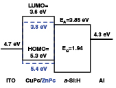
In this work, the VOC appears to depend strongly on the thickness of the organic layers. It certainly cannot be explained by the MIM model. In order to further explore this, device performance can be further analysed according to the energy diagram as shown in figure 6, where the energy levels of CuPc (HOMO ~ 5.3, LUMO ~ 3.6) [40], ZnPc (HOMO ~ 5.4, LUMO ~ 3.8) [67] and a-Si : H [EA(a-Si : H) = 3.85, Eg(a-Si : H) = 1.94] [27] were inferred from the literature. If an organic model is taken, p-type Pc might act as an electron donor in the device, while the relative electron affinity levels determine that the a-Si : H layer acts as an electron acceptor. Subsequently, photo-generated excitons were dissociated at the interface between the Pcs and the a-Si : H, followed by negative electric charges transferring from the Pcs to silicon and a positively charged layer being registered in the Pcs films, as described in the literature [68]. From figure 6, it can be seen that the difference of the HOMO levels between ZnPc and CuPc is quite small. Therefore, the VOCs of the corresponding devices are expected to have a comparable trend with thickness. In fact, the VOC from the ZnPc/α-Si : H device is slightly higher than that from the CuPc/α-Si : H device. This is consistent with experimental observations except for very thin Pcs devices, such as 30 nm. However, the VOCs of the Pcs/a-Si : H hybrid heterojunction cells are much lower than the energy difference between the HOMO of the Pcs and the EA of the α-Si : H and they are unexpectedly related to the thickness of the organic layer. This phenomenon was reported in our previous work [27], but it cannot be fully explained using this organic model.
Figure 6. Energy level diagram of devices studied in this work. CuPc (solid line); ZnPc (dashed line).
Download figure:
Standard image High-resolution image
The difference in the excitation mechanism of organic or inorganic material may be taken into account. Under illumination, the electron–hole pairs created in the dyes are intrinsically excitonic (Frenkel excitons), whereas electron–hole pairs in the α-Si : H are probably unbound due to exciton (Wannier excitons) binding energies under 0.1 eV[69] and hence are relatively easy to dissociate than in the organic dyes. However, there is a difference in charge carrier transportation properties: Pcs are p-type semiconductor with a hole mobility in the range 10–2 and the intrinsic Si mainly transports electrons with an electron mobility of about 10–1 cm2 V−1 s−1. In this case, both holes and electrons may not easily cross the organic/Si junction. A charge accumulation at the junction may be formed. Having analysed the I–V curves under illumination, the space charge limited currents were observed. These need further theoretical investigation into their influence on the device action and will be worked on in the future.
This work is a preliminary attempt to build a hybrid device and to gain a basic understanding of optoelectronic properties of thin silicon film deposited on organic films. All devices are simple structures and therefore the contacts at the electrodes have not been optimized. It may form future work along with further investigation.
4. Conclusions
The application of hybrid structures between organic and inorganic films in PV devices has attracted considerable attention in recent years, but the physical mechanism is still under debate. This work offers a preliminary investigation into the preparation of novel but simply structured hybrid heterojunction solar cells. The devices consist of chemically stable and optoelectronically active Pc dyes and an intrinsic a-Si : H film. Three device configurations, i.e. CuPc/a-Si : H, ZnPc/a-Si : H, and CuPc/ZnPc/a-Si : H, were fabricated along with ITO and Al as bottom and top electrodes. PV performances were discussed, which were found to be closely related to the thickness of the organic layers. The effect was particularly strong with the open circuit voltages. The photocurrents of hybrid devices responded the best in the blue spectral range mainly from the a-Si : H layer. The organic layer certainly removed the top 'dead layer' in amorphous silicon. However, the unbalanced charge transport between the MPc and a-Si : H layers appears to limit transport efficiency of the charge carriers and hence the carrier collection at the electrode. It offers a new direction for future device optimization.
Acknowledgments
The authors would like to thank Professor Bryce Richards and Mr David Ross for their kind assistance with some measurements. This work was funded in part by the ISTCP China (2008DFA61420), the NSF China (21174016) and RFDP (No. 20120009110031). HZ would like to thank the China–Scotland Higher Education Research Partnership for the PhD Studies and for sponsoring his short term visit to Heriot–Watt University.