
Abstract
Dual-junction solar cells formed by a GaAsP or GaInP top cell and a silicon bottom cell seem to be attractive candidates to materialize the long sought-for integration of III–V materials on silicon for photovoltaic applications. One of the first issues to be considered in the development of this structure will be the strategy to create the silicon emitter of the bottom subcell. In this study, we explore the possibility of forming the silicon emitter by phosphorus diffusion (i.e. exposing the wafer to PH3 in a MOVPE reactor) and still obtain good surface morphologies to achieve a successful III–V heteroepitaxy as occurs in conventional III–V on germanium solar cell technology. Consequently, we explore the parameter space (PH3 partial pressure, time and temperature) that is needed to create optimized emitter designs and assess the impact of such treatments on surface morphology using atomic force microscopy. Although a strong degradation of surface morphology caused by prolonged exposure of silicon to PH3 is corroborated, it is also shown that subsequent anneals under H2 can recover silicon surface morphology and minimize its RMS roughness and the presence of pits and spikes.
Export citation and abstract BibTeX RIS
1. Introduction
Multijunction solar cell (MJSC) architectures have demonstrated a tremendous potential for achieving very high photovoltaic (PV) conversion efficiencies. Commercial MJSC designs are based on the growth of complex structures of III–V semiconductors on a substrate material, namely germanium, which is both costly and scarce [1]. These problems have spurred an active quest for alternative substrates, where silicon (Si) emerges as a natural choice as a result of its abundance and relatively low cost. Interesting efforts in this direction were carried out in the past and have re-emerged strongly in the last decade. One of the most promising approaches so far investigated is based on the use of a GaP nucleation layer to achieve a defect-free III–V template on Si [2–4]. On this template, GaAsP graded buffers can be grown onto which GaInAsP top cells of the adequate bandgap can be integrated, thus forming a GaAsP/Si [5, 6] or a GaInP/Si [7] dual-junction solar cell (DJSC).
Although several research groups have been working in the development of this structure, their efforts have been mostly directed towards the optimization of key steps in the epitaxial growth of III–V compounds on silicon, such as the nucleation layer, the graded buffer and the top subcell [4, 5, 8]. Their main target has been the minimization and confinement of crystal defects in the structure, without paying much attention to the consequences of such processes on the silicon substrate (which eventually will act as the bottom subcell of the DJSC). However, the formation of a high-quality bottom cell will be crucial for obtaining a highly efficient multijunction structure [9]. In this work we will review key aspects to form an optimized bottom subcell for the hybrid III–V-on-Si DJSC, as is the preparation of the silicon substrate for subsequent III–V growth, and also the formation of an emitter with an adequate thickness and dopant concentration.
A careful preparation of the substrate surface is required for growing a defect-free III–V nucleation layer on a group IV substrate. If no preparation of the substrate is carried out, then antiphase disorder and other crystal defects are produced in the layer. Therefore, the nucleation layer will grow exhibiting poor morphology—3D growth and island formation—and thus will limit the quality of the active layers of the device [10, 11] or, in extreme cases, will hamper further growth. In order to guarantee an optimal silicon surface for subsequent epitaxial growth, wafers are generally submitted to an initial thermal annealing [10, 11]. In this way, Si substrates are usually heated (between 800 °C and 1150 °C) under hydrogen. The purpose of this treatment is twofold: (1) to ensure a deoxidized Si surface and (2) to promote the formation of a double atomic step surface.
Another aspect which has to be taken into account for obtaining an optimal bottom subcell is the formation of the emitter with an adequate thickness and dopant concentration. One alternative to create it is by homoepitaxial growth of silicon on the Si substrate. This implies either the need for a special metal organic vapour phase epitaxy (MOVPE) reactor able to grow both group IV and III–V compounds (i.e. specially designed to minimize cross-contamination and carryover effects), or to grow the structure in a two-step process (i.e. taking the samples out of the reactor after Si growth, cleaning the reactor, and loading again for III–V growth). The use of homoepitaxial growth of Si has demonstrated to be a beneficial factor in the production of high-quality GaP-on-Si layers [2, 4], though, as discussed, introduces an additional degree of complexity in the epitaxial process. A simpler alternative would be to mimic what is done in conventional MJSC technology on germanium substrates, where the bottom subcell emitter is formed by the diffusion of phosphorous (P), resulting from the pyrolysis of phosphine (PH3). In this respect, it should be noted that several groups have also reported high-quality GaP layers without homoepitaxial silicon buffers [3, 5].
The goal of this work is to explore the possibility of forming the silicon subcell emitter by phosphorus diffusion (i.e. exposing the wafer to PH3) and still obtain good surface morphologies to achieve a successful III–V heteroepitaxy as occurs in conventional III–V-on-germanium solar cell technology. A first question to answer is then what emitter design (in terms of thickness and doping concentration) is needed in a silicon subcell of a III–V-on-Si solar cell. Figure 1 represents a set of simulations in which by colour plots, the evolution of short circuit current density (JSC), open circuit voltage (VOC) and fill factor (FF) of the silicon subcell under 1 sun AM1.5D illumination in a GaAsP/GaP/Si structure are represented as a function of emitter doping and thickness. These calculations have been carried out using the numerical simulator SILVACO ATLAS, which provides the capability of simulating different technological processes (such as phosphorus diffusion in Si), different structural defects and different materials, including both group IV and III–V semiconductors. Additional details about this simulation can be found elsewhere [12].

Figure 1. Colour plots for silicon subcell parameters as a function of emitter doping and thickness. (a) Short circuit current density (JSC); (b) open circuit voltage (VOC); (c) fill factor (FF).
Download figure:
Standard image High-resolution imageFigure 1 shows that thick highly doped emitters (right upper corner in the maps) will give rise to lower JSC and, to a lesser extent, VOC, whilst thin lightly doped emitters (left lower corner in the maps) will lose VOC and FF. Therefore, good emitter designs avoid these two extreme regions and (approximately) lie on the top left corner of the maps. In this respect, the shallow (<0.25 µm) and highly doped (>1019 cm−3) emitters typically associated to diffusion are optimum designs to implement a high quality emitter for the silicon subcell.
In our case, the fabrication of III–V-on-Si solar cells is carried out in a MOVPE reactor. Therefore, the thickness and dopant concentration of the diffused emitter will be determined by the concentration of precursors in the reactor and the thermal load associated with the process. At the initial stage of the emitter formation several phosphorus compounds may coexist depending on the process followed and the temperature reached: atomic or molecular P desorbed from the reactor walls and/or other heated parts (susceptor, exhaust, etc); PH3 intentionally injected and the by-products of its pyrolysis (PH2, etc). All these compounds interact with the wafer surface to provide a final coverage of P dimers and some displacement of silicon dimers (roughening). As a result of a certain phosphorus surface coverage at the temperatures used for the MOVPE process, diffusion of P into the wafer takes place.
In order to evaluate which are the annealing conditions required to form the shallow and highly doped emitter discussed above, some simulations have been carried out. The simulations have been calculated following the models described in [13], where an extra injection of vacancies and interstitials was considered to account for the particular conditions of P diffusion into silicon in a MOVPE environment. For each simulated diffusion profile, the emitter depth and the average emitter doping have been calculated, considering a base doping level of 2 × 1015 cm−3. Figure 2 shows the expected emitter depth as a function of diffusion temperature and time. Likewise, the evolution of the emitter doping level with diffusion temperature and time is shown in figure 3.
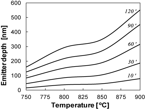
Figure 2. Simulated emitter depths as a function of diffusion temperature and time.
Download figure:
Standard image High-resolution image
Figure 3. Average emitter doping level in the silicon subcell as a function of diffusion temperature and time.
Download figure:
Standard image High-resolution imageAs is shown in figure 2, an emitter with the desirable depth (70–250 nm)—not too thin to avoid shunting problems and not too thick to keep efficiency high according to figures 1(a) to (c)—can be obtained when working within a temperature range of 750–900 °C using annealing times between 10 and 120 min. In this work we will study the parameter space of temperatures ranging from 800 to 875 °C and annealing times between 10 and 120 min. Combinations with lower (higher) temperatures and longer (shorter) times are, in principle, possible though seem impractical for a MOVPE environment and lie out of the typical conditions used for the initial thermal treatments usually reported for silicon wafers before III–V growth [10, 11], as mentioned above. According to figure 3, no further constraints on this parameter space are forced by the doping of the emitter since even the lower temperatures explored lead to the formation of highly doped emitters (doping level higher than 1 × 1019 cm−3 in all cases).
A side effect of the formation of the emitter by P diffusion is the roughening of the Si surface. It has been described that exposure of Si (1 0 0) surfaces to PH3 may result in roughening of the surface due to Si hydridation and subsequent dimmer displacement [14, 15]. Other authors have even observed the formation of SiP compounds when Si samples are annealed under high PH3 partial pressures [16]. However, it has been also reported that these compounds are no longer present when the PH3 flow was reduced during the cool down of the sample. The effect of surface roughening on the morphology of subsequently grown layers has been widely studied, though contradictory visions are reported in the literature. On the one hand, it is well known that roughening and foreign species can limit the quality of the active layers of the device, due to the poor quality of the epitaxial growth. On the other hand, a beneficial effect of the substrate roughness on the nucleation layer quality has been observed, since roughened substrates present larger surface areas and higher densities of irregularly oriented dangling bonds as compared with conventional substrates [17]. Soga et al found that preheating Si substrates to 900 °C under PH3 and H2 was essential to obtain a smooth GaP nucleation layer [8]. Moreover, Andre et al found that not only wafer misorientation, but also PH3 preflow are used for reducing the film cracking density and to promote the growth of single crystal [18]. In addition, Takano et al have described the influence of PH3 preflow on the initial MOVPE growth of the GaP nucleation layer, when short flushes of PH3 are used prior to GaP epitaxy [14]. In essence, all these works confirmed that despite Si surface becoming rough during the PH3 preflow, the P- prelayer, formed during such PH3 preflow was necessary to obtain a flat GaP surface. However, it is worth noting that the PH3 concentration and the time exposure had a determining effect on the nucleation layer morphology: the use of an adequate PH3 concentration and time exposure will lead to a quick GaP island coalescence and hence to the formation of a continuous layer; in contrast, prolonged exposure of the surfaces to phosphine may result in island faceting and therefore, in poor GaP layer quality [14]. In summary, these authors support the beneficial effect of a short (and lowly concentrated) PH3 flush in attaining a high-quality GaP layer, due to the formation of a P prelayer, which favours the GaP two-dimensional growth.
In our target application, the roughening problem will be more severe though; since, as we have shown above, relatively high temperatures (800–875 °C approximately) together with long exposure times (up to 120 min) under high concentrations of PH3 will be needed to reach the diffusion depths (70–250 nm) required for the formation of a good emitter for the Si subcell (figure 2). Consequently, this work aims to analyse the effect on Si substrate surface morphology of the environment and conditions in the MOVPE reactor during the emitter formation (i.e. after long and highly concentrated PH3 exposures). Therefore, in our quest of obtaining an optimized bottom subcell for a hybrid III–V-on-Si DJSC, we will assess whether or not it is possible to form the emitter by P diffusion, while maintaining a high-quality surface morphology on the silicon wafer.
With this purpose, in an initial set of experiments, wafers have been annealed in hydrogen under different conditions belonging to the parameter space determined to assess the sole effect of H2 on substrate surface morphology. Temperature, time and reactor pressure have been varied to assess the impact of each variable on the surface reconstruction (table 1). In a second set of experiments, wafers have been annealed under PH3 for different times, temperatures and partial pressures (table 2). Finally, an additional experiment, including both PH3 annealing and H2 annealing has been carried out (table 3) to assess the impact of a combined treatment on the surface morphology.
Table 1. Description and roughness parameters of the first batch of experiments where wafers were annealed under pure hydrogen. An as-received wafer has also been included for comparison.
| Sample | Treatment | Temperature (°C) | Time (min) | Pressure (mbar) | RMS (nm) | Skewness | Kurtosis |
|---|---|---|---|---|---|---|---|
| 4.a | As-received | — | — | — | 0.46 | −1.32 | 5.38 |
| 4.b | H2 anneal | 830 | 60 | 100 | 0.38 | −0.72 | 4.08 |
| 4.c | H2 anneal | 830 | 60 | 900 | 0.31 | −0.38 | 6.67 |
| 4.d | H2 anneal | 875 | 60 | 100 | 0.18 | 0.07 | 3.14 |
| 4.e | H2 anneal | 830 | 120 | 100 | 0.19 | 0.04 | 3.33 |
| 4.f | H2 anneal | 875 | 120 | 900 | 0.20 | 0.02 | 3.15 |
Table 2. Description and roughness parameters of the second batch of experiments where wafers were annealed under hydrogen mixed with different partial pressures of PH3.
| Sample | Treatment | Temperature (°C) | Time (min) | PH3 pressure (mbar) | Pressure (mbar) | RMS (nm) | Skewness | Kurtosis |
|---|---|---|---|---|---|---|---|---|
| 4.a | As-received | — | — | — | — | 0.46 | −1.32 | 5.38 |
| 5.a | PH3 anneal | 830 | 60 | 32.1 | 900 | 2.23 | −0.05 | 3.02 |
| 5.b | PH3 anneal | 800 | 60 | 32.1 | 900 | 1.17 | 0.21 | 2.98 |
| 5.c | PH3 anneal | 855 | 60 | 32.1 | 900 | 4.52 | 1.99 | 7.55 |
| 5.d | PH3 anneal | 830 | 60 | 3.2 | 100 | 0.30 | −0.73 | 4.24 |
| 5.e | PH3 anneal | 830 | 10 | 32.1 | 900 | 0.48 | 0.95 | 6.39 |
| 5.f | PH3 anneal | 855 | 30 | 32.1 | 900 | 0.99 | 0.38 | 3.19 |
Table 3. Description and roughness parameters of the third batch of experiments where wafers were first annealed under hydrogen mixed with 32.1 mbar of PH3 and then annealed under pure hydrogen.
| Sample | MOVPE treatment | RMS (nm) | Skewness | Kurtosis | Simulated emitter depth (nm) | |
|---|---|---|---|---|---|---|
| PH3 annealing | H2 annealing | |||||
| 6.a | 30 min 830 °C | — | 0.73 | 0.26 | 3.21 | 95 |
| 6.b | 30 min 830 °C | 60 min 830 °C | 0.38 | 0.07 | 3.70 | 121 |
| 6.c | 30 min 830 °C | 60 min 875 °C | 0.29 | −0.03 | 2.66 | 145 |
| 6.d | 10 min 875 °C | — | 0.54 | 0.44 | 4.88 | 59 |
| 6.e | 10 min 875 °C | 60 min 875 °C | 0.29 | 0.10 | 3.13 | 110 |
| 6.f | 10 min 875 °C | 90 min 875 °C | 0.29 | 2 × 10⁻³ | 3.09 | 128 |
2. Experimental
The experiments were carried out in a horizontal AIX200/4 MOVPE reactor. The carrier gas was Pd-purified H2, and the P precursor used was high-purity PH3. The substrates used for this work were p-type boron-doped Czochralski Si wafers, oriented (1 0 0) with a 2° miscut to the nearest (1 1 1) plane. Wafers were deoxidized using an HF dip, before loading them into the MOVPE reactor. The surface morphology of the samples was examined by atomic force microscopy (AFM) using a Digital Instruments-Multimode IIIa microscope working in tapping mode and the resulting AFM scans were processed using a free software tool [19]. All AFM scans presented in this work are topography scans of 2 × 2 µm in size. Phosphorus diffusion profiles have been measured by means of electrochemical capacitance-voltage profiling (ECV) using NH4F/HF as electrolyte. The emitter depth was estimated by an extrapolation from a fit of the ECV profiles using a complementary-error function (for two steps annealing) or Gaussian function (for single-step annealing).
3. Results and discussion
Table 1 and figure 4 summarize the results of the first batch of experiments where samples were annealed under H2 at different temperatures, times and reactor pressures. An as-received sample (4.a) was measured as a benchmark for morphology.
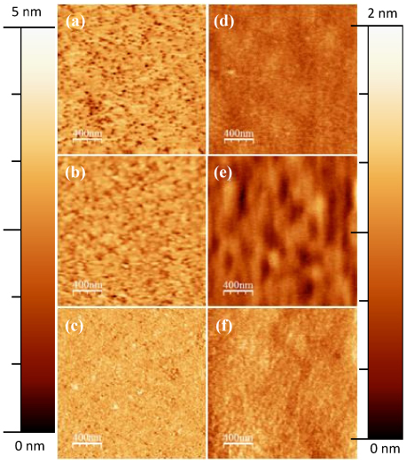
Figure 4. Comparison of AFM topography scans of Si wafers annealed in hydrogen atmosphere as a function of the annealing conditions as indicated in table 1. An as-received wafer has been included for comparison (a). Left and right-hand side scans are represented in a different Z scale.
Download figure:
Standard image High-resolution imageAs shown by table 1 the results of this sample suggest that as-received wafers are essentially flat surfaces (i.e. have a moderate RMS roughness below 0.5 nm) with a noteworthy presence of quite deep pits. The presence of pits is indicated by a negative surface skewness far from the equilibrium value of 0 and the depth of the pits is suggested by the value of surface kurtosis, which is significantly larger than the equilibrium value of 3.
The sample annealed at 830 °C during 60 min under H2 (sample 4.b), shows an improvement of surface RMS roughness, skewness and kurtosis (which evolve towards their equilibrium values) indicating that the annealing under hydrogen improves the flatness of the surfaces and diminishes the presence and depth of the pits. The impact of H2 pressure in the reactor can be assessed comparing sample 4.b with sample 4.c. Moderately lower surface roughness and skewness are obtained at higher pressures further indicating a smaller number of pits in sample 4.c. However, the larger value of kurtosis in 4.c could indicate that increasing the pressure is not enough to get rid of the deepest pits. The impact of a large increase in the annealing temperature can be ascertained by comparing sample 4.b (830 °C) and 4.d (875 °C). The RMS (root mean square roughness) value of sample 4.d reaches an extremely low value and the skewness and kurtosis approach to their equilibrium values of 0 and 3, respectively.
The effect of time can be evaluated comparing samples 4.b (60 min) and 4.e (120 min). The surface parameters of sample 4.e are excellent with a very low RMS roughness, skewness and kurtosis around their equilibrium values. Finally, to further substantiate the importance of the time variable, sample 4.f accounts for the effect of a moderate increase in temperature to 875 °C and an increase in H2 pressure to 900 mbar, while maintaining the long duration of the anneal of 120 min. As shown by table 1, the roughness parameters of samples 4.e (830 °C, 100 mbar) and 4.f (875 °C, 900 mbar) are virtually identical, suggesting a minor effect of the temperature (in this range) and pressure. In summary, from this study, we can conclude that the sufficiently long H2 anneals at temperatures in the range 830–875 °C will improve the surface morphology of silicon wafers producing extremely flat surfaces free of pits, the H2 pressure being a second-order parameter in terms of its influence in this process.
In order to assess the impact of the PH3 environment required to form the emitter on surface morphology, silicon wafers were annealed at high temperatures including in the gas mixture for different partial pressures of PH3. Table 2 and figure 5 summarize the results of these experiments. In order to make more evident the effect of PH3 on the surface morphology, again an as-received wafer has been included in the set for comparison.

Figure 5. Comparison of AFM topography scans of Si wafers annealed under H2 mixed with different partial pressure of PH3, as a function of the annealing conditions as indicated in table 2. Left and right side scans are represented in a different Z scale.
Download figure:
Standard image High-resolution imageAs shown by table 2, the presence of PH3 during the annealing leads to an important roughening of the Si surface. However, this degradation is deeply affected by the annealing conditions. The role of the annealing temperature can be assessed by comparing samples 5.b (800 °C), 5.a (830 °C) and 5.c (855 °C). Increasing the temperature has a significant effect on the RMS roughness, which increases markedly for each step in temperature, reaching roughness values up to ten times higher than the one measured in the as-received wafer. Furthermore, the depth of the pits increases with the temperature, especially for the highest temperature (5.c at 855 °C), since the value of surface kurtosis becomes greater than the equilibrium value of 3. The effect of pressure can be evaluated comparing samples 5.a (900 mbar) and 5.d (100 mbar). As shown by table 2, a reduction of the annealing pressure leads to a significant reduction of the roughness. However, the value of the skewness and kurtosis are far from their equilibrium values indicating that, even at low pressure, PH3 has some impact on surface roughening. Finally, the impact of a shorter annealing time can be ascertained by comparing samples 5.c (60 min.) and 5.f (30 min.). The sample annealed at 855 °C for 30 min. (sample 5.f), shows an improvement of surface RMS roughness, skewness and kurtosis (which evolve towards their equilibrium values) indicating that the exposure time has an important effect on the surface roughness. A similar behaviour is observed in samples 5.a (60 min) and 5.e (10 min) annealed at a slightly lower temperature of 830 °C. Again, the reduction of the time exposure leads to a reduction of the RMS roughness, with both kurtosis and skewness around their equilibrium values, in any case better than those of as-received wafers.
On the one hand, according to table 2, PH3 exposure must be minimized (i.e. reduce the temperature, decrease the pressure and the time exposure) for obtaining a smooth silicon surface. On the other hand, according to ECV measurements (not shown here) the use of weak PH3 anneals leads to emitter depths thinner than 70 nm (too shallow and probably prone to showing low shunt resistance). Therefore, with the goal of achieving optimal emitter depths, while preserving the surface morphology, a third batch of experiments was conducted. In this case, the formation of the emitter by exposing wafers to a high PH3 partial pressure was followed by a H2 annealing intended to recover damaged surface morphology. Obviously, the last step will also modify the P profile in the structure, since the H2 anneal will favour the P to further penetrate into the silicon substrate. In this sense an additional column, which shows the emitter depth for each sample, has been included in table 3. The junction depths have been calculated from simulated P profiles [13]. As shown in table 3, the emitter is moderately increased with the addition of the hydrogen anneal, obtaining emitter depths in the optimum range, according to figure 1.
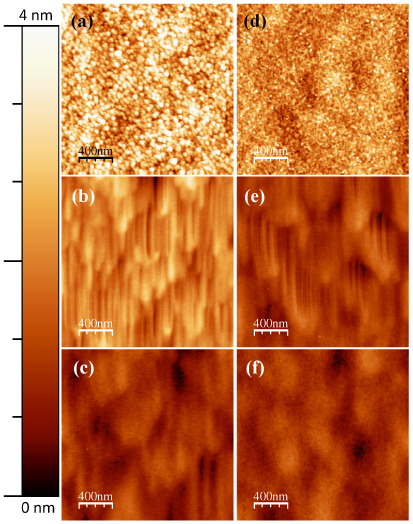
Table 3 and figure 6 summarize the results of the third set of experiments. Firstly, silicon wafers were annealed at high temperatures under 32.1 mbar of PH3. Afterwards, with the aim of recovering the silicon surface morphology (degraded during the formation of the emitter), samples were annealed at high temperatures under hydrogen. The role of the final H2 annealing process can be easily assessed by comparing the pair of samples: (1) 6.a (no final H2 annealing) and 6.b (final H2 annealing for one hour); and (2) 6.d (no final H2 annealing) and 6.e (final H2 annealing for one hour). The addition of the hydrogen annealing has an evident effect on recovering the RMS roughness and the skewness of the sample after the formation of the emitter. The effect of the H2 annealing temperature can be evaluated by comparing samples 6.b (830 °C) and 6.c (875 °C). The sample annealed at higher temperature shows an improvement of surface RMS roughness, skewness and kurtosis (which evolve towards their equilibrium values) indicating that the annealing under hydrogen improves the flatness of the surfaces and diminishes the presence and depth of the pits. Finally, the effect of the final H2 annealing time can be ascertained by comparing samples 6.e (60 min.) and 6.f (90 min.). The surface parameters of both samples are excellent with a very low RMS roughness, skewness and kurtosis approaching their equilibrium values of 0 and 3, respectively. Both samples are virtually identical, suggesting a minor effect of the time (at this temperature).
Figure 6. AFM topography scans of the experiments summarized in table 3. All scans are represented in the same Z scale.
Download figure:
Standard image High-resolution image
As we have mentioned before, the goal of this work was to explore the possibility of forming an optimum silicon subcell emitter by P diffusion, while preserving a good surface morphology to achieve a successful III–V heteroepitaxy on silicon.
We have reported so far that an emitter of an adequate thickness (according to figure 1) can be formed by P diffusion (table 2), though a degraded Si morphology is then obtained. We have also demonstrated that it is possible to reconstruct the Si morphology through the introduction of a subsequent hydrogen anneal (after a short exposure to phosphine). This fact is corroborated by the RMS reduction shown in table 3. Moreover, we have reported that this step (i.e. hydrogen anneal) will help the phosphorous to drive-in and thus, the emitter depth will be increased as compared to single PH3 annealed samples (6.a and 6.d), as shown in table 3.
Finally, in order to fully assess the impact of the emitter formation conditions on the solar cell performance, we have calculated the short circuit current density (JSC), open circuit voltage (VOC) and fill factor (FF) of the silicon subcell under 1 sun AM1.5D illumination in a GaAsP/GaP/Si structure, for each Si sample included in table 3. More details of the cell structure and the parameters used for the simulations are given in [12].
According to table 4, the increase of the emitter depth (as a result of the P drive-in) does not have a substantial impact on the silicon solar cell performance. This is primarily due to the fact that, in a tandem configuration, only the long-wavelength part of the spectrum reaches the bottom subcell. Then, the light absorption of the thin silicon emitters is greatly reduced, and the short circuit current attained by the bottom subcell is basically determined by the cell base properties. Thus, small differences in the emitter depth do not have a big influence on the cell performance.
Table 4. Simulation of silicon subcell parameters for samples included in table 3.
| Sample | Emitter depth (nm) | Emitter doping (cm−3) | Jsc (mA cm−2) | Voc (mV) | FF (%) |
|---|---|---|---|---|---|
| 6.a | 95 | 3.97 × 10¹⁹ | 12.250 | 520.179 | 80.678 |
| 6.b | 121 | 1.56 × 10¹⁹ | 12.236 | 514.236 | 80.497 |
| 6.c | 145 | 9.29 × 10¹⁸ | 12.232 | 514.240 | 80.497 |
| 6.d | 59 | 6.89 × 10¹⁹ | 12.249 | 520.347 | 80.684 |
| 6.e | 110 | 1.13 × 10¹⁹ | 12.236 | 513.786 | 80.482 |
| 6.f | 128 | 7.92 × 10¹⁸ | 12.237 | 514.491 | 80.506 |
However, the slight decrease in Voc observed for samples 6.b, 6.c, 6.e, and 6.f, can be explained by the modification of the diffusion profiles as the result of the drive-in step [13]. In those samples, the doping near the surface is reduced (as compared to samples 6.1 and 6.c), decreasing the electric field which drives the photogenerated carriers towards the pn junction leading to a slightly enhanced carrier recombination at the front surface.
In summary, we can conclude that the formation of the emitters through the combined treatment is the best method so far for obtaining high-quality devices, since the H2 annealing after the P diffusion will recover the surface morphology of silicon wafers producing extremely flat surfaces free of pits. Although a slight reduction of Voc is expected for those emitters, its design is still in the optimum range, according to figure 1. The implementation of GaP nucleation layers on these surfaces is underway and will be reported in future works.
4. Conclusions
With the final target of obtaining a high-quality hybrid III–V-on-Si DJSC, in this study we have reviewed a strategy to form an optimized emitter for the bottom subcell. This process requires both an adequate preparation of the substrate surface for subsequent III–V epitaxial growth, and also the formation of an emitter with an adequate thickness and dopant concentration. In this sense, we have analysed the evolution of the surface morphology during the formation of the emitter, which, in our case, occurs by P diffusion. Although the exposure of substrates (before growth) to a short PH3 flush has been proven to be beneficial for obtaining a high-quality GaP morphology; we have demonstrated that the effect of long PH3 exposures at temperatures ranging from 800–875 °C (required for obtaining a deep enough emitter) will lead to an important degradation of the surface. However, we have proven that using a combined treatment consisting of PH3 exposure (P diffusion) followed by a H2 annealing, leads us to obtain an optimum emitter (shallow and highly doped) while preserving high-quality morphology for following heteroepitaxial growth.
Acknowledgments
AFM images included in this work were taken at the National Centre for Electronic Microscopy (Universidad Complutense de Madrid). This work was supported by FP7 Program of the European Union through project NGCPV(283798) and by the Spanish Ministerio de Economía y Competitividad through project with reference TEC2012-37286.