
Abstract
We report the synthesis and transfer of epitaxial germanane (GeH) onto arbitrary substrates by electrochemical delamination and investigate its optoelectronic properties. GeH films with thickness ranging from 1 to 600 nm (2–1000 layers) and areas up to ∼1 cm2 have been reliably transferred and characterized by photoluminescence, x-ray diffraction, and energy-dispersive x-ray spectroscopy. Wavelength dependent photoconductivity measurements on few-layer GeH exhibit an absorption edge and provide a sensitive characterization tool for ultrathin germanane materials. The transfer process also enables the possibility of integrating germanane into vertically stacked heterostructures.
Export citation and abstract BibTeX RIS
Graphene, a single atomic sheet of carbon, has been a revolutionary material with unique properties for electronics, spintronics, and surface science [1–5]. Recently there has been intense interest in two-dimensional (2D) materials beyond graphene that have a native band gap and stronger spin–orbit coupling [6–9]. Germanane, the germanium analog of graphane (i.e. hydrogen-terminated graphene), is a new 2D material with a direct band gap that can be tuned via surface covalent functionalization [9–11]. Additionally, germanane is air stable and has a high predicted mobility of 18 000 cm2 V−1s−1 at room temperature, making it extremely promising for electronic and optoelectronic applications [9]. Specifically, the combination of high mobility, non-zero bandgap, and low dimensionality are advantageous for short channel field effect transistors with high on-off ratios and low quiescent currents [7]. Furthermore, germanane's large spin–orbit coupling makes it possible to explore novel physical phenomena such as quantum spin Hall effect at room temperature [12–14].
It is worthwhile to compare the general band structure characteristics of germanane (with hydrogen termination) and germanene (without hydrogen termination) [15–18]. Germanene has a band structure similar to graphene, with Dirac cones at the ±K points of the Brillouin zone and conduction electron Bloch states composed primarily of pz orbitals. The main difference is the larger spin–orbit coupling due to the larger mass of Ge compared to C, producing a spin–orbit gap of ∼24 meV at the ±K points (compared to 24–50 μeV for graphene) [19]. When a germanene sheet is modified by covalently bonding hydrogen atoms to both sides, one obtains germanane (GeH). The covalent bonding involves the pz orbitals of the Ge atom and causes a substantial gap to open at the ±K points, so the electron transport properties are no longer determined by the Bloch states involving the pz orbitals. Instead, transport is determined by the Bloch states near the Γ point, with a conduction band derived from s-orbitals and a valence band derived from the px and py orbitals [9]. The direct gap band structure is rather similar to conventional semiconductors such as GaAs with an s-orbital conduction band and p-orbital valence bands, except that the pz orbital is removed by the covalent bonding with the hydrogen. Thus, numerous properties of conventional direct gap semiconductors will translate to germanane, including spin-selective optical selection rules, contact hyperfine coupling in the conduction band, and spin–orbit splitting in the valence band [20].
Recently, large area germanane films have been synthesized by growing Zintl-phase CaGe2 thin films on Ge(111) wafers by molecular beam epitaxy (MBE) [21] or substrate reaction [22, 23], followed by chemical processing in acid solution to convert the CaGe2 into hydrogen-terminated germanane (GeH). In order to utilize this material for electronic devices, it is necessary to transfer the GeH film to an insulating substrate to prevent parallel conduction paths. In addition, a transfer process will allow the integration of GeH into vertically stacked heterostructures with other 2D materials. In this paper, we report the synthesis and transfer of large area epitaxial GeH by electrochemical delamination (i.e. 'bubble transfer') and demonstrate electron transport and photoconductivity. We are able to reliably transfer films up to ∼1 cm2, which is limited by the size of our sample holder. The photoluminescence (PL) spectra and the x-ray diffraction (XRD) scans remain largely unchanged by the transfer process, indicating that the optical and bulk structural properties are maintained. Furthermore, energy-dispersive x-ray spectroscopy (EDS) shows no residual electrolyte (within measurement sensitivity) remaining from the transfer process. We investigate electron transport and photoconductivity by transferring to insulating substrates and depositing metallic electrodes through shadow masks. In particular, photoconductivity of few-layer GeH exhibits an absorption edge as a function of wavelength as expected for a semiconductor. Because most other techniques for characterizing germanane have required thick films or bulk crystals, the demonstration of photoconductivity measurements on few layer GeH is very important for the further optimization and development of ultrathin germanane materials.
Growth of epitaxial germanane films
The first step is to deposit Zintl-phase CaGe2 films on Ge(111) substrates by MBE in an ultrahigh vacuum (UHV) chamber (base pressure of 2 × 10⁻¹⁰ Torr) [21]. Elemental germanium and calcium are evaporated from thermal effusion cells with high purity germanium (99.9999% from Alfa Aesar) and calcium (99.99% from Sigma Aldrich) source materials. Growth rates are determined by a quartz deposition monitor. All films are grown on p-type Ge(111) single-side polished wafer with thickness of ∼0.350 mm and orientation tolerance of 0.5° (University Wafer). The starting 2'' diameter wafer is cleaved into smaller pieces (up to 10 mm) which then undergo chemical etching to remove surface oxides and metal contaminants. Etching involves a sequence of steps beginning with immersion in a solution of H2O:NH4OH (10:1) for 60 s, followed by H2O:H2SO4 (10:1) for 60 s. Finally the substrate is submerged into 30% H2O2 aqueous solution for 60 s to produce a thin protective oxide layer. The wafers are then rinsed with DI water, blown dry with nitrogen gas, and inserted into the UHV chamber where a 30 min anneal at 650 °C removes the protective oxide layer.
The MBE growth of CaGe2 is performed at 750 °C in an adsorption-limited growth regime. The typical Ca:Ge flux ratio is held slightly above 0.5 for slightly Ca-rich conditions. Excess Ca atoms are either re-evaporated or possibly reacted into the Ge substrate. Assuming that the growth rate is determined by the Ge flux, typical growth rates for the CaGe2 are ∼3 Å min−1 for films thinner than 200 nm and ∼15 Å min−1 for films thicker than 200 nm. In both cases, sharp and streaky reflection high energy electron diffraction patterns are obtained [21]. These patterns indicate that the CaGe2 film maintains epitaxial orientation with the Ge(111) substrate.
Subsequently, the CaGe2/Ge(111) is removed from vacuum and submerged in a 37% solution of HCl for 24–48 h at −40 °C depending on sample thickness. This de-intercalates the calcium atoms and replaces them with covalently bonded hydrogen atoms to produce 2D stacked layers of GeH [9, 21, 22]. As shown in figure 1, the Ge atoms form a buckled honeycomb structure and each of the Ge atoms is bonded to a hydrogen atom for sp3 hybridization. The (0001) lattice parameter is expanded during the de-intercalation of CaGe2 to GeH by 7% [9], leading to slightly thicker GeH films. Unless otherwise noted, the reported thicknesses are those of the final GeH film. For films less than 50 nm, thicknesses were determined by AFM, whereas for thicker films, the reported values are based on growth rates. Details of the MBE growth and chemical processing are provided in [21].
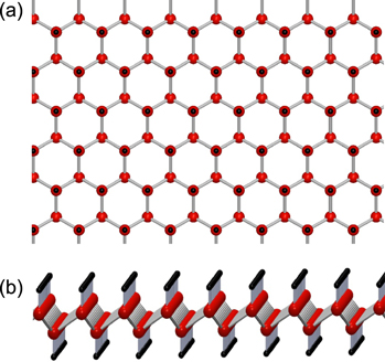
Figure 1. (a) Top view of GeH, (b) side view of GeH.
Download figure:
Standard image High-resolution imageThe morphology of the resulting GeH film depends on the sample thickness. Samples thinner than 10 nm (∼18 layers) have relatively smooth surfaces with island or terrace formation due to the substrate miscut [21], while samples thicker than 50 nm (∼88 layers) display the formation of cracks (figure 3(c)). These cracks form during the growth of the CaGe2 film and are probably related to the 1% lattice mismatch with the Ge(111) substrate [23], where defects and dislocations form beyond a critical thickness in order to relax substrate-induced strain. While there is considerable room to improve the quality of the films, we note that the large area transfer has worked reliably in spite of these imperfections.
Large area transfer
To realize germanane-based electronic devices, it is necessary to transfer the GeH film to an insulating substrate. Our initial attempts at transferring the GeH film included mechanical exfoliation using various tapes and polydimethylsiloxane stamping procedures. However, these methods resulted in low yield and small flake size (<10 μm). A popular method for transferring large area 2D films is to support the film with polymer and etch away the underlying substrate, which is commonly used to remove copper foil from CVD graphene [24]. However, we are not aware of a selective etch that differentiates between GeH and Ge. Therefore, we focus our attention to electrochemical delamination based on water electrolysis, i.e. bubble transfer [25, 26], which has been effective for transferring other 2D materials.
Figure 2(a) illustrates the main steps for the transfer and figures 2(b)–(e) are photographs taken during the process. Beginning with a GeH film on a p-type Ge (111) substrate (figure 2(b)), we spin coat the sample with polymethylmethacrylate (PMMA) at 2000 rpm for 45 s and then bake at 50 °C for 2 h. The PMMA coating of GeH provides structural support during the delamination process. To facilitate detachment during the water electrolysis, the PMMA on the edge of the substrate is removed with acetone. Then, we dip the PMMA/GeH/Ge(111) cathode and a graphite anode into a 1 M NaOH aqueous solution and slowly increase the current at a typical rate of ∼0.01 A s−1 (figure 2(c)) until the PMMA/GeH starts to detach. The current produces H2 bubbles at the interface between the PMMA/GeH and the Ge(111) due to water reduction (2H2O + 2e− → H2 (g) + 2OH− (aq)). The hydrogen bubbling time necessary to detach the PMMA/GeH layer from the Ge substrate depends on the size of the film and the current applied. Typically, after approximately 10 s of bubbling, the PMMA/GeH layer floats to the top of the NaOH solution (figure 2(d)). The corresponding electrolyte voltage is approximately 5 V with a current of ∼0.06 A for a 1 cm2 sample. The PMMA/GeH is then moved to a bath of de-ionized (DI) water for 15 min to remove the remaining electrolytes from the sample. After cleaning, we transfer the PMMA/GeH layer to the desired substrate and bake on a hot plate at 50 °C for 10 min to help remove the interfacial water layer. The residual PMMA is removed by immersing the transferred sample in acetone at 50 °C for 30 min, followed by an isopropanol rinse for 1 min to remove the acetone. Finally, we dry the sample with nitrogen gas. Figure 2(e) shows a transferred film with a size of several mm.
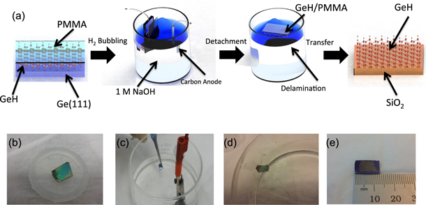
Figure 2. (a) Schematic of the transfer process, (b) optical image of PMMA/GeH/Ge(111), (c) optical image of the electrochemical cell, (d) optical image of the floating PMMA/GeH film (e) optical image of GeH transferred to SiO2.
Download figure:
Standard image High-resolution imageWe have successfully transferred GeH films between 1 nm (2–3 layers) and 600 nm (∼1000 layers) thicknesses to arbitrary substrates. Figure 3 shows optical and scanning electron microscope (SEM) images of 5 nm (∼9 layers) GeH films transferred to a SiO2(300 nm)/Si substrate. The optical image (figure 3(a)) shows a continuous large area of GeH. The upper right corner of the image shows the edge of the film, which is visible due to color contrast with the bare substrate. The SEM image (figure 3(b)) shows continuous regions larger than ∼1 mm and separated by tears, which produce enhanced contrast between the substrate and film. The continuous regions are typically larger and exhibit fewer features (supplementary figure S4). For the thicker GeH, we observe similar cracking before transfer (figure 3(c)) and after transfer (figure 3(d)), which shows that the morphology is conserved.
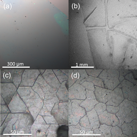
Figure 3. (a) Optical micrograph of 5 (∼9 layers) nm GeH transferred to SiO2, (b) SEM image of 5 nm (∼9 layers) GeH transferred to SiO2, (c) optical micrograph of 600 nm (∼1000 layers) as grown GeH on Ge(111), (d) optical micrograph of 600 nm (∼1000 layers) GeH transferred to SiO2.
Download figure:
Standard image High-resolution imageTo determine the effect of the transfer on the quality of GeH films, we perform a series of characterization measurements before and after transferring. To minimize substrate-related effects, we transfer the GeH film from its original Ge(111) substrate to another Ge(111) substrate. The out-of-plane lattice spacing was analyzed using XRD on a 600 nm (∼1000 layers) GeH film. Before transfer, we observe a peak at 2θ = 15.8° which corresponds to the GeH layer spacing of 5.7 Å. This is in agreement with XRD characterizations of bulk GeH crystals, where synchrotron-based measurements of the pair distribution function have confirmed the buckled honeycomb structure of the GeH layers [10]. As shown in figure 4(d), the position and line width of the GeH peak are preserved after transfer, indicating that the transfer does not produce major changes to the crystal structure.
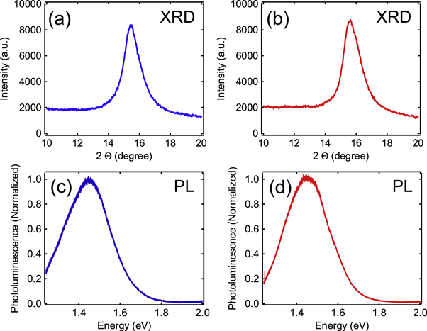
Figure 4. (a) XRD of as-grown 600 nm (∼1000 layers) GeH film, (b) XRD of transferred 600 nm (∼1000 layers) GeH film, (c) PL of as-grown 600 nm (∼1000 layers) GeH film, (d) PL of transferred 600 nm (∼1000 layers) GeH film.
Download figure:
Standard image High-resolution imageTo investigate the effect of transfer on optical properties, we perform PL spectroscopy at low temperatures (10 K). PL is performed using a 532 nm laser excitation (1 mW, 20 μm spot size) and the spectra are captured using a 0.5 m Czerny–Turner spectrometer with a liquid nitrogen cooled CCD camera (Princeton Instruments). A white light source (tungsten lamp modeled as a blackbody) is used to calibrate and correct for the wavelength dependence of the detector efficiency. The PL spectrum before transfer exhibits a peak at ∼1.45 eV, (figure 4(c)) which is consistent with previous reports of PL on epitaxial GeH [22]. After transfer, the PL spectrum again exhibits a peak at ∼1.45 eV and the intensity is not degraded (figure 4(d)). Notably, we did not observe PL at ∼1.9 eV, which is reported to occur in the presence of oxidation [22]. This suggests that the transfer of GeH does not promote oxidation and preserves the optical quality.
Finally, we have examined the possible contamination of a 600 nm thick sample during the transfer using EDS spectroscopy (Oxford Instruments) in an SEM at 20 kV (1000 nm penetration depth). The spectrum before transfer shows a strong Ge signal and no observable Ca and O signals (supplementary figure S1). In addition, we performed low energy 10 kV (340 nm penetration depth) EDS and observed some surface oxidation (supplementary figure S2). The Cl remaining in the material after deintercalation is about 7%, similar to what has been reported previously [10, 22]. After transfer, the 20 kV EDS spectra was free of Na and O signals (supplementary figure S1). This confirms that the transfer introduces little or no contamination (below detection limits) to the GeH film.
Electron transport and photoconductivity
To investigate the electrical and photoconductive properties of GeH films on the SiO2(300 nm)/Si substrate, we deposit metallic electrodes through shadow masks. For thicker films (>50 nm), we utilize a shadow mask with fine features in order to have a continuous conduction channel in between the cracks. Figure 5(a) is an optical microscope image of a 600 nm (∼1000 layers) GeH film with Au/Ti electrodes separated by 20 μm. Dc photoconductivity is measured by applying a voltage between the drain and source and measuring the current under illumination by a 635 nm laser. A factor 50 increase in current from dark is observed when illuminated by 0.014 W cm−2 635 nm light (supplementary figure S3).
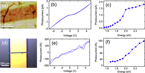
Figure 5. (a) Optical micrograph of a 600 nm (∼1000 layers) GeH device, (b) bias dependence of photocurrent for the 600 nm (∼1000 layers) GeH device illuminated by 540 nm light, (c) wavelength dependence of photocurrent at 5 V bias for the 600 nm (∼1000 layers) GeH device, (d) optical micrograph of a 5 nm (∼9 layers) GeH device, (e) bias dependence of photocurrent for the 5 nm (∼9 layers) GeH device illuminated by 540 nm light, (f) wavelength dependence of photocurrent at 5 V bias for the 5 nm (∼9 layers) GeH device.
Download figure:
Standard image High-resolution image
Wavelength dependent ac photoconductivity measurements are performed using pulsed laser excitation (150 fs, 76 MHz repetition rate) from a Ti:sapphire oscillator (700–960 nm wavelength range) or optical parametric oscillator (520–740 nm wavelength range). The laser beam is maintained at a power of 1.0 mW and has a beam diameter of ∼2 mm. The beam is incident on the device without a focusing lens, thereby producing a broad illumination with an intensity of ∼0.03 W cm−2. The beam is chopped at a frequency of 493 Hz and the resulting photocurrent is pre-amplified and measured by lock-in detection. All photocurrent measurements are performed at room temperature.
Figure 5(b) shows the photocurrent of a 600 nm (∼1000 layers) GeH device as a function of bias voltage for a laser wavelength of 540 nm. The bias voltage is ramped from 0 to +5 V to −5 to 0 V to detect possible hysteretic effects as a function of bias voltage. The photocurrent versus voltage curve exhibits no hysteresis and is slightly nonlinear. We investigate the wavelength dependence of the photocurrent by adjusting the laser wavelength and repeating this measurement every 20 nm. Figure 5(c) summarizes the wavelength dependence by plotting the photocurrent at +5 V bias. At low photon energies, there is little photocurrent because the photon energy is below the band gap. As the photon energy is increased, more photons are absorbed and the photocurrent increases. This behavior is typical of a semiconductor, where the absorption rapidly increases as the photon energy exceeds the band gap and is similar to recent measurements on bulk germanane crystals [27]. We note that this photocurrent spectrum is also similar to previous optical reflectance spectroscopy performed on epitaxial GeH/Ge(111) [28].
To develop few-layer germanane devices, we next focus our attention on the characterization of thin GeH films (∼5 nm). However, initial studies on thin GeH failed to produce consistent results, and we hypothesized that the problem was oxidation of the CaGe2 film due to air exposure prior to de-intercalation. To prevent such difficulties, we added an extra step in the synthesis procedure, in which we grew 5 nm Ca followed by 10 nm Fe to cap the CaGe2 film prior to de-intercalation. This minimizes the potential oxidation of the CaGe2 layer as the sample is transferred in air from the MBE chamber to the HCl solution [22]. Once inside the HCl solution, the Fe and Ca layers are dissolved, and then the underlying CaGe2 film is de-intercalated to produce GeH. After de-intercalation, we performed EDS to ensure that the capping layer is completely removed (below detection limit) and the CaGe2 is converted to GeH (supplementary figure S7). Because these films are continuous, we deposit larger metallic electrodes of width 400 μm and separated by a 20 μm gap. Figure 5(d) is an optical microscope image of such a device with GeH film thickness of 5 nm (∼9 layers). Figure 5(e) shows the photocurrent of this device as a function of bias voltage under laser illumination at 540 nm. There is an order of magnitude less photocurrent for this device compared to the thick GeH and the signal is approaching the level of the noise. Compared to the thicker films which exhibit nonlinear IV (figure 5(b)), the thinner films have more linear IV characteristics and the photoconductivity can be quantified by a linear fit. The linear IV may be associated with improved contacts due to the Fe capping procedure (i.e. reduced oxidation as confirmed by EDS in supplementary figure S7), but systematic studies have not yet been performed. The photocurrent spectrum shown in figure 5(f) displays the expected behavior for a semiconductor, with low photocurrent at low photon energies and an increase of photocurrent with increasing photon energy. Although the absorption edge appears to have shifted to slightly higher energies compared to the thick device (figure 5(c)), the overall features of the photoconductivity spectra are similar. We have also observed photoconductive signals in 1 nm (2–3 layers) GeH films (see supplementary Materials).
The ability to measure these weak photoconductivity signals is very important for the optimization of few-layer germanane films. Up until now, the most important materials characterizations such as XRD and PL could only be applied to thick GeH films due to the lack of measurable signal in the thinner films. Now with the photoconductivity measurement, we have a means of characterizing the electronic and optical properties of few-layer germanane and can use this information to optimize the material synthesis procedures.
Conclusion
We developed the synthesis and transfer of GeH onto arbitrary substrates. This is an important advance, as the transfer of GeH enables the fabrication of electronic devices on insulating substrates, optical studies on transparent substrates, as well as the creation of vertically stacked 2D heterostructures. We verified that the structural and optical properties of thick GeH films are largely unchanged by the transfer process with PL and XRD. Additionally, the transfer process does not contaminate the thick GeH films with residual electrolytes (within measurement sensitivity), verified with EDS spectroscopy. Once transferred, GeH films were fabricated into two-terminal devices to allow transport measurements and photoconductivity measurements. The photoconductivity of both thick and few-layer GeH indicates an absorption edge as a function of wavelength, as expected for a semiconducting material. The photoconductivity measurements on few-layer GeH are particularly important for the further optimization and development of ultrathin germanane materials due to its high sensitivity. These results represent a major advance toward the realization of electronic and optoelectronic applications in this emerging 2D material.
Acknowledgments
We thank Scott Crooker for technical assistance. WA, PMO and DJO developed the transfer process and subsequent characterization. WA performed the device fabrication and electrical measurement. EJB performed the photoconductivity measurements. Research at UC Riverside was primarily supported by ARO (W911NF-11-1-0182) and UC Labs (12-LR-239009). Research at Ohio State was primarily supported by NSF MRSEC (DMR-1420451) and NSF (DMR-1310661). We also acknowledge the support of C-SPIN, one of six centers of STARnet, a Semiconductor Research Corporation program sponsored by MARCO and DARPA.