


The unprecedented wide bandgap tunability (∼1 eV) of AlxIn1-xAsySb1-y lattice-matched to GaSb enables the fabrication of photodetectors over a wide range from near-infrared to mid-infrared. In this paper, the valence band-offsets in AlxIn1-xAsySb1-y with different Al compositions are analyzed by tight binding calculations and X-ray photoelectron spectroscopy measurements. The observed weak variation in valence band offsets is consistent with the lack of any minigaps in the valence band, compared to the conduction band.
AlxIn1-xAsySb1-y materials lattice-matched to GaSb substrates can be utilized to fabricate photodetectors that operate from near-infrared to mid-infrared photodetectors owing to a wide compositional tuning of the bandgap energy. Previously, a miscibility gap1–3 prevented the development of AlxIn1-xAsySb1-y devices with high Al concentrations. Vaughn et al. demonstrated a technique to circumvent this limitation with digital alloy structures with an Al fraction up to 35% by using periodic cells composed of a few monolayers (ML) of the binary materials, AlAs, AlSb, InAs, and InSb.4,5 Maddox et al. extended this method to cover the entire direct bandgap range of compositions (to x ≈ 80%).3 This digital alloy material has been used to fabricate a staircase avalanche photodiode (APD)6 and separate absorption, charge, and multiplication (SACM) APDs that operate at 1550 nm with excess noise comparable to that of Si.7 To date, there have been few studies on the material characteristics of AlxIn1-xAsySb1-y. For electronic and optoelectronic devices, the relative conduction and valence band offsets at the interfaces of different compositions are important parameters. In fact, a possible origin of low excess noise in some digital alloys seems to be the emergence of sizable minigaps inside one carrier band, which may eventually be connected to the variation in the corresponding band offsets.8 Recent electroreflectance measurements on AlxIn1-xAsySb1-y indicate that the valence band offsets are very low.9 In this paper, a first-principles study based on an empirical tight binding model and X-ray photoelectron spectroscopy (XPS) are used to determine the bandgap discontinuities.
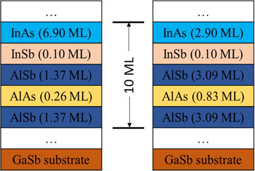
Figure 1 shows the periodic structures of the digital alloy AlxIn1-xAsySb1-y considered in this paper. Figures 1(a) and 1(b) show the structures for the compositions x = 30% and x = 70%, respectively. The AlxIn1-xAsySb1-y digital alloy is fabricated by periodically stacking 4 binary materials: InAs, InSb, AlSb, and AlAs; each period consists of 10 monolayers (ML). The Al composition, x, and As composition, y, are controlled by the thicknesses of the binary layers. In this paper, the band structures of AlxIn1-xAsySb1-y with x varying from 0% to 80% are analyzed. The layer structure of a unit cell for each composition is provided in Table I. The thicknesses of the layers are designed to achieve a lattice match to the GaSb substrate. The material growth rate was carefully designed to approach the targeted thickness.
Lattice structure for (a) x = 30% and (b) x = 70% AlxIn1-xAsySb1-y digital alloys.
Lattice structure for (a) x = 30% and (b) x = 70% AlxIn1-xAsySb1-y digital alloys.
AlxIn1-xAsySb1-y digital alloy nominal monolayer fractions for various binary alloy constituents in a unit cell, for x varying from 0% to 80%.
| x = 0% | x = 10% | x = 20% | x = 30% | x = 40% | x = 50% | x = 60% | x = 70% | x = 80% | |
|---|---|---|---|---|---|---|---|---|---|
| InAs (ML) | 9.68 | 8.82 | 7.90 | 6.90 | 5.90 | 4.90 | 3.90 | 2.90 | 1.90 |
| InSb (ML) | 0.32 | 0.19 | 0.10 | 0.10 | 0.10 | 0.10 | 0.10 | 0.10 | 0.10 |
| AlSb (ML) | … | 1.00 | 0.95 | 1.37 | 1.77 | 2.20 | 2.63 | 3.09 | 3.57 |
| AlAs (ML) | … | … | 0.10 | 0.26 | 0.46 | 0.60 | 0.74 | 0.83 | 0.87 |
| AlSb (ML) | … | … | 0.95 | 1.37 | 1.77 | 2.20 | 2.63 | 3.09 | 3.57 |
Since the layer thicknesses in AlxIn1-xAsySb1-y digital alloy are so thin, the electron wave function has a significant overlap with that in adjacent layers. Consequently, this is not a multiquantum well material. Yet, it does have periodicity, and therefore, it is not bulk material. It is a new material, which has its own features. In this work, an environment-dependent empirical tight-binding model is used to calculate the band structure. In this model, neighboring atoms, bond angles, and bond lengths are considered; the empirical parameters were obtained by iteratively adjusting with hybrid density functional (HSE06) results. This model has been verified in many different material structures including the InAlAs digital alloy,2,8 group IV and III–V heterojunctions, and ultrathin Si and MoS2 layers.10–12 The empirical parameters have been published in the literature.11 Since the lattice has periodicity along the growth direction, supercells are chosen consistent with the smallest repeatable units. Since we need to maintain the total thickness of each period at 10 ML, the monolayer numbers for the individual layers are not necessarily integers, which means that the adjacent layers overlap. This raises the issue that the lateral distribution of atoms is somewhat random. In order to reduce the calculation time, we simplify the lateral atomic distribution to be regular and thus reduce the size of the supercell.
At first, supercells for AlxIn1-xAsySb1-y digital alloy are taken in the form shown in Fig. 2, where x = 40%, 60%, and 80% are shown as examples.

Supercell for AlxIn1-xAsySb1-y digital alloy with a decimal number of monolayers in each period.
Supercell for AlxIn1-xAsySb1-y digital alloy with a decimal number of monolayers in each period.
The supercell consists of 100 atoms. Fractional monolayers overlap with adjacent layers as illustrated in Fig. 2 with the dashed rectangular boxes.
Strain is also included in this model. The lattice constant, a, Poisson ratio, Di, and shear moduli, are provided in Table II. Lateral and vertical lattice constants ( and ) can be calculated using the following equations:8
where i denotes the adjacent material and is the layer thickness. From Table I, it can be seen that in the AlxIn1-xAsySb1-y digital alloy, each period is primarily composed of InAs and AlSb. Therefore, for simplification, the influence of InSb and AlAs on the lattice parameters is ignored.
Lattice constant a (in angstrom), shear moduli G, and for InAs, InSb, AlAs, and AlSb used in this work.11,13,14
| A | |||||||
|---|---|---|---|---|---|---|---|
| InAs | 6.06 | 1.088 | 1.587 | 0.674 | 2.306 | 0.570 | 2.487 |
| InSb | 6.48 | 1.080 | 1.261 | 0.698 | 1.785 | 0.600 | 1.920 |
| AlAs | 5.66 | 0.854 | 2.656 | 0.616 | 3.207 | 0.550 | 3.361 |
| AlSb | 6.14 | 0.990 | 1.763 | 0.641 | 2.372 | 0.550 | 2.530 |
E-k relationships along the [001] direction for x varying from 0% to 80% have been calculated, and x = 0%, 40%, and 80% are shown in Fig. 3 as examples. The calculation of different samples uses the same vacuum level and the same energy coordinate. The band structure results indicate that the valence band maximum (VBM) is relatively independent of x.
![FIG. 3. E-k relationships along the [001] direction for AlxIn1-xAsySb1-y samples with (a) x = 40%, (b) x = 60%, and (c) x = 80%.](https://aipp.silverchair-cdn.com/aipp/content_public/journal/apl/115/12/10.1063_1.5107516/3/m_122105_1_f3.jpeg?Expires=1717040354&Signature=VV7HwRT3pwNxDnkntuBu8YWGQaWZ0o3pOG5r0rM8I1jiG-K3sVnwnXwQXdhQO4PDymNdk7tAUheXSlDJDasv3AIgaG6ZuM65e9JiyGdFQ7h1Sos-q4l4NoDKJcEUp528JLkLwfSDlLMSamoMmejCehlSF4u-hJW5oxobOTiEE8AW3xpS6xwC4gTKQg~vFBTrR-QNx2OP0uI6FSWYirGnDQCJBHgp~-InHLh9oGYvNRTnAW68TPzMno8wZEsdpM7dgKfIG1fE4jdCbY1pJA23PPsYFaY1lKncUFST-kYeIBytAGxqiuCR49fAUy1b3qaelh2NK9TwSeoy0T6Ei5N0Zg__&Key-Pair-Id=APKAIE5G5CRDK6RD3PGA)
E-k relationships along the [001] direction for AlxIn1-xAsySb1-y samples with (a) x = 40%, (b) x = 60%, and (c) x = 80%.
E-k relationships along the [001] direction for AlxIn1-xAsySb1-y samples with (a) x = 40%, (b) x = 60%, and (c) x = 80%.
The valence band maximum and conduction band minimum (CBM) values are plotted as dashed and solid curves, respectively, in Fig. 4. From 0% to 80%, the increase in the valence band maximum is <0.1 eV. Linear fitting is used to illustrate the trend for the CBM and VBM. The slopes for the VBM and CBM are 0.09 and 1.52, respectively.

Tight binding calculating results for the valence band maximum (VBM) and conduction band minimum (CBM) and XPS measurement results for VBM of the AlxIn1-xAsySb1-y digital alloy.
Tight binding calculating results for the valence band maximum (VBM) and conduction band minimum (CBM) and XPS measurement results for VBM of the AlxIn1-xAsySb1-y digital alloy.
In order to determine the effect of the lateral randomness caused by fractional monolayers in the supercell on the band structure, we considered the configuration with no overlap between adjacent layers, i.e., whole numbers of monolayers, as shown in Table III. The band structure of AlxIn1-xAsySb1-y with x = 60% was re-calculated. The supercell and E-k relationship are shown in Fig. 5. Comparing Fig. 5(b) with Fig. 3(b), it is found that the band structure does not change a lot. The valence band maximum shifts upward ∼0.06 eV, and the conduction band minimum shifts downward ∼0.08 eV. We conclude that the lateral randomness caused by adjacent layer merging is relatively insignificant.
AlxIn1-xAsySb1-y digital alloy layer structures in a unit cell for x varying from 0% to 80% with the whole number of monolayers adding up to 10 ML.
| x = 0% | x = 10% | x = 20% | x = 30% | x = 40% | x = 50% | x = 60% | x = 70% | x = 80% | |
|---|---|---|---|---|---|---|---|---|---|
| InAs (ML) | 10 | 9 | 8 | 7 | 6 | 5 | 4 | 3 | 2 |
| InSb (ML) | … | … | … | … | … | … | … | … | … |
| AlSb (ML) | … | 1 | 1 | 1 | 1 | 2 | 2 | 3 | 4 |
| AlAs (ML) | … | … | … | 1 | 1 | 1 | 1 | 1 | 1 |
| AlSb (ML) | … | … | 1 | 1 | 2 | 2 | 3 | 3 | 3 |

Ultimate condition of lateral randomness; (a) single column simplification of supercell with x = 60% and (b) E-k relationship.
Ultimate condition of lateral randomness; (a) single column simplification of supercell with x = 60% and (b) E-k relationship.
In order to confirm the AlxIn1-xAsySb1-y digital alloy band offset with different x values, X-ray photoelectron spectroscopy (XPS) measurements were carried out using a PHI VersaProbe III system with a monochromatic Al k-alpha X-ray source (1486.7 eV). The photoelectron energy spectrum includes the information from the atoms in the top 10 nm depth of the material, which involves several periods of the digital alloy. The equipment has in situ sputtering capability, which has been used to remove the surface oxide, in order to ensure that the spectrum is collected from the correct layers. The valence band maximum values were fixed at the intersection point of the linear extrapolation of the leading edge and the valence band spectra baseline (a 0.05 eV spectrum resolution was used). In this work, Sb 4d cathode-luminescence was selected to obtain the valence band offset, between Alx1In1-x1Asy1Sb1-y1 and Alx2In1-x2Asy2Sb1-y2 by using the Kraut model,15–17 which is given by the following equation, which calculates energy shifts upon altering compositions from (Alx1,Asy1) to (Alx2,Asy2) first in the Sb 4d state and then in the VBM,
where denotes the peak in , which can vary from sample to sample owing to differences in the surface potential, as shown in Fig. 6(a). Figure 6(b) shows the intersectional points for x varying from 0% to 80%.

Normalized XPS data of (a) Sb4d peaks and (b) VBM for AlxIn1-xAsySb1-y with x varying from 0% to 80%.
Normalized XPS data of (a) Sb4d peaks and (b) VBM for AlxIn1-xAsySb1-y with x varying from 0% to 80%.
The valence band offsets for different compositions have been calculated and are plotted in Fig. 4 as solid circles, •. Consistent with the band structure calculations, the valence band discontinuity is relatively independent of the composition. It follows that the bandgap discontinuity is primarily in the conduction band.
The big variation in the conduction band offset and small variation in the valence band offset between the two binary constituent alloys (mainly between AlSb and InAs18) are consistent with the observed minigaps inside the conduction band and their absence in the valence band (Figs. 3 and 5) and also the band offset variation between AlInAsSb with different Al compositions. A detailed transport model will be necessary hereafter to connect these band minigaps with the charge transmission, which depends on various details such as scattering potential, transport and tunneling effective masses, and phonon energies.
In conclusion, the valence band offset between materials lattice matched to GaSb with x varying from 0% to 80% has been found to be nearly 0 by using tight binding calculations and XPS measurements. The change in bandgap energy with the Al fraction, therefore, is primarily due to the conduction band offset.
This work was supported by the Army Research Office (No. W911NF-17-1-0065) and DARPA (No. GG11972.153060).

