


The properties of molecular beam epitaxy-grown InSb1−xBix alloys are investigated. Rutherford backscattering spectrometry shows that the Bi content increases from 0.6% for growth at 350 °C to 2.4% at 200 °C. X-ray diffraction indicates Bi-induced lattice dilation and suggests a zinc-blende InBi lattice parameter of 6.626 Å. Scanning electron microscopy reveals surface InSbBi nanostructures on the InSbBi films for the lowest growth temperatures, Bi droplets at intermediate temperatures, and smooth surfaces for the highest temperature. The room temperature optical absorption edge was found to change from 172 meV (7.2 μm) for InSb to ∼88 meV (14.1 μm) for InSb0.976Bi0.024, a reduction of ∼35 meV/%Bi.
III-V-bismide alloys have attracted attention due to their interesting band structure, significant Bi-induced band gap reduction, and increase in spin-orbit splitting which make them suitable for optoelectronic devices operating in the near- and mid-infrared regions.1–4 While III-SbBi alloys have been less extensively researched than III-AsBi alloys, interest in them is increasing, particularly for high power lasers and detectors in the important 2–5 and 8–14 μm ranges. There are only a few recent reports on the growth and properties of GaSbBi and related alloys, targeting the lower wavelength of these ranges.5–11 Meanwhile, InSbBi was one of the first dilute bismides to be explored.12–16
In 1969, InSbBi alloys with a few percent Bi were identified by Jean-Louis and Hamon as a potentially important alternative to HgCdTe for long wavelength infrared sources and detectors operating in the 8–14 μm atmospheric transmission window.12 Their pioneering work on InSbBi alloys involved investigations of bulk Czochralski-grown crystals. The lattice parameter was found to increase linearly with Bi content up to the maximum achieved of 2.4% of the anion sublattice.14 Optical absorption showed that the InSbBi single crystals exhibit respective band gap reduction of ∼38 and ∼30 meV/% Bi at 4 and 300 K.12,13 Rather surprisingly, these optical results have not been clearly reproduced for epitaxial material in spite of many reports on InSbBi over the last four decades.
In fact, reports on the band gap reduction for epitaxial InSbBi are rather scarce. They include a recent report of ∼6 meV reduction for 0.4 atomic % Bi content; this low value was attributed to low substitutionality of Bi on group V lattice sites.5 In a report on metal organic vapor phase epitaxy (MOVPE)-grown InSbBi, promising indications of band gap reduction were provided by photoresponse measurements, but experimental data on the composition were absent.17,18 The same study reported lattice contraction with respect to InSb, a result recently also obtained for InSbBi grown by liquid phase epitaxy (LPE) and molecular beam epitaxy (MBE).5,17,19 This contrasts with both the predictions of theoretical calculations20 and also the lattice expansion found in the Czochralski-grown samples and other InSbBi alloy samples grown by MBE21 and MOVPE.22
In this letter, we report the structural and optical properties of InSbBi alloys grown by MBE. The InSbBi epilayers were grown by solid-source MBE on 100 nm InSb buffer layers on undoped InSb(001) substrates. The Bi beam equivalent pressure flux was set to approximately 3.3 × 10⁻⁸ mbar using the beam monitoring ion gauge. The InSbBi epilayers were grown to a thickness of ∼300–400 nm at a fixed growth rate of nominally 0.4 μm h−1 using substrate temperatures ranging from 200 to 350 °C. Growth temperatures were determined using a pyrometer down to 240 °C. This enabled thermocouple readings to be calibrated and the calibration was extrapolated down to 200 °C.
The Bi content and lattice constant of the InSbBi films were determined using RBS with 3.72 MeV He2+ ions and HRXRD using a Philips X'Pert diffractometer equipped with a monochromatic Cu Kα1 x-ray source (λ = 0.15406 nm). The surface morphology and composition of the InSbBi alloys was investigated by JEOL JSM-7001F FESEM with EDS and an Asylum research MFP-3D AFM in AC mode (tapping mode). The surface composition was also probed by hard x-ray photoemission spectroscopy (HAXPES) measurements. A photon energy, hν, of 4 keV was used and the instrumental broadening was 0.45 eV. Transmittance measurements were performed using a Bruker Vertex 70 V Fourier-transform infrared spectrometer, using a liquid nitrogen-cooled HgCdTe detector.
The morphology of the InSbBi films was investigated using SEM and EDS (Fig. 1). The sample grown at the lowest temperature (200 °C) shows the formation of nanostructures (NS) on top of the InSbBi film. The sample grown at 225 °C exhibits both NS and droplets. At intermediate growth temperatures (250–325 °C), the samples only show droplet formation on the InSbBi films and for growth at 350 °C the film is droplet-free. The film grown at 350 °C has a very smooth surface with root mean square roughness of ∼0.8 nm on a 5 μm by 5 μm AFM image. EDS indicates that the NS are InSbBi with Bi content that varies from NS to NS within the range of 19–43 atomic %. For the sample grown at 200 °C, the In and Sb contents in the different NS vary in the ranges 41%–27% and 45%–30%, respectively, and in approximately inverse proportion to the Bi content suggesting that Bi occupies both In and Sb lattice sites. Bi is well known to exist in both trivalent and pentavalent states. The steeper dependence of Sb content on Bi concentration than for the In content implies that about four fifths of the Bi in the NS is on the anion sublattice and one fifth on the cation sublattice. EDS also indicates that the droplets are pure Bi. The height of InSbBi NS is ∼70 nm as measured by AFM and cross-sectional SEM.

SEM images of InSbBi samples grown at 200, 225, 300, and 350 °C, showing rectangular InSbBi nanostructures and Bi droplets. The insets show SEM images of the same samples after HCl etching, indicating the removal of Bi droplets by etching.
SEM images of InSbBi samples grown at 200, 225, 300, and 350 °C, showing rectangular InSbBi nanostructures and Bi droplets. The insets show SEM images of the same samples after HCl etching, indicating the removal of Bi droplets by etching.
The surface of all the samples was etched by HCl as an additional means of distinguishing between metallic droplets and InSbBi NS. The insets of Fig. 1 show the SEM images of the samples after HCl etching. The sample grown at 200 °C did not change significantly with etching; the InSbBi NS were not etched away. For the samples grown at between 225 and 325 °C, the droplets identified by EDS as being Bi were removed by HCl etching. Similarly shaped NS have previously been reported at the surface of InSbBi alloys grown by MOVPE but were identified by EDS as being BiSb rather than the InSbBi found here.23,24
The Bi content in InSbBi cannot be determined accurately from the XRD calculated lattice constant by using Vegard's law, due to the lattice parameter of zinc-blende InBi being experimentally unknown. Therefore, RBS was employed and simulated using the SIMNRA code.25 Fig. 2 shows the InBi mole fraction variation along the film thickness for films grown at 200 (solid black line) and 350 °C (dashed red line). The sample grown at 350 °C shows uniform Bi incorporation of 0.6% of the anion sublattice, whereas the sample grown at 200 °C shows a clear change in Bi incorporation along the film thickness, varying from 1.0% in a ∼70 nm-thick “bottom” layer closest to the buffer layer to 2.4% in a ∼150 nm-thick “middle” layer. As shown in Fig. 2, there is also a ∼60 nm-thick region of the film in which the Bi content changes from 1.0 to 2.4%. At the surface, the InBi mole fraction increases drastically and reaches ∼30%, resulting from the Bi content in InSbBi NS. The inset of Fig. 2 shows the lattice constant from the XRD (as discussed below) as a function of Bi content from RBS measurements.

The variation of RBS-determined InBi mole fraction through the films grown at 200 (solid black line) and 350 °C (dashed red line). The inset shows the lattice parameters measured by XRD as a function of the Bi content from RBS.
The variation of RBS-determined InBi mole fraction through the films grown at 200 (solid black line) and 350 °C (dashed red line). The inset shows the lattice parameters measured by XRD as a function of the Bi content from RBS.
For the highest growth temperature, RBS channeling measurements indicate that 96% of the Bi is substitutional on the anion sublattice throughout the film; so for a total Bi content of 0.60%, the substitutional Bi content is 0.58%. For the samples grown at lower temperatures, the RBS data indicate that they consist of three layers with different Bi content as depicted in the inset of Fig. 3 which shows a schematic diagram of the InSbBi epilayers on InSb substrate. The “top layer” corresponds to either InSbBi NS or Bi droplets at the surface while the “middle” and “bottom” layers are InSbBi films of various Bi content as shown in Fig. 3 as a function of growth temperature.

The Bi content from RBS as a function of growth temperature in the “top,” “middle,” and “bottom” layers of the InSbBi epilayers represented, respectively, by squares, circles, and triangles. The inset shows a schematic diagram of the InSbBi films. The RBS Bi content is expressed as a proportion of the anion sublattice and uses the left axis. The Bi contents for the “top” layer InSbBi NS and Bi droplets should be taken as a qualitative indication of the trend of decreasing amount of Bi at the surface with increasing growth temperature rather than as quantitative values, as the RBS analysis assumes a planar compact film throughout. EDS indicates that the true Bi content of the NS is ∼30 atomic % and for the Bi droplets is 100%. The Bi:In ratio from HAXPES is shown by the stars and uses the right axis.
The Bi content from RBS as a function of growth temperature in the “top,” “middle,” and “bottom” layers of the InSbBi epilayers represented, respectively, by squares, circles, and triangles. The inset shows a schematic diagram of the InSbBi films. The RBS Bi content is expressed as a proportion of the anion sublattice and uses the left axis. The Bi contents for the “top” layer InSbBi NS and Bi droplets should be taken as a qualitative indication of the trend of decreasing amount of Bi at the surface with increasing growth temperature rather than as quantitative values, as the RBS analysis assumes a planar compact film throughout. EDS indicates that the true Bi content of the NS is ∼30 atomic % and for the Bi droplets is 100%. The Bi:In ratio from HAXPES is shown by the stars and uses the right axis.
The Bi content in the InSbBi NS for the samples grown at 200 and 225 °C is found to be ∼30% when expressed as a proportion of the anion sublattice, corresponding to ∼15 atomic %. However, these values obtained from analysis of the RBS data assuming a uniform compact film only give a qualitative description of the trend of reducing surface Bi content with increasing growth temperature. The true Bi content of the NS and droplets is best estimated from the aforementioned EDS. The amount of Bi in droplets on the surface diminishes as the growth temperature is increased and disappears completely at 350 °C. The near-surface Bi/In ratio, averaging over regions with and without NS and Bi droplets, was determined from HAXPES of the In 4d and Bi 5d core levels. The curve-fitting, using Voigt functions, included the indium and bismuth oxide surface components, and their contribution was omitted from the Bi:In ratio. The Bi:In ratio was corrected to account for differences in orbital cross-sections and reflects the composition within the first 10–15 nm from the surface. For growth at 200 °C, the Bi:In ratio is close to 1 due to the presence of NS containing up to 40 atomic % Bi and regions of InSbBi films with Bi anion substitution of 2.4% and below. As the growth temperature is increased, the HAXPES Bi:In ratio decreases corresponding to greater Bi desorption and decreasing Bi droplet coverage. For the highest growth temperature of 350 °C, where NS and Bi droplets are absent the surface Bi:In ratio is consistent with the RBS-determined Bi content of the InSbBi film of 0.6%.
The Bi contents in the “middle” and “bottom” layers of the sample grown at 225 °C are, respectively, 0.9% and 1.3% (0.85% and 1.2% if only substitutional Bi is considered). The films grown at intermediate temperatures (250–325 °C) have thin (∼60–75 nm) “middle” layers with Bi content varying from 3.6% to 8.0% and ∼300 nm-thick “bottom” layers with low Bi content of ∼0.5% to 0.8%. Channeling RBS shows that all the samples are of high crystallinity with greater than 95% of Bi atoms on substitutional group V lattice sites in the bottom layers and also in the middle layers for growth at 200 and 225 °C, but only ∼25% Bi substitutionality in the middle layers for growth between 250 and 325 °C.
The RBS evidence of a transition between the bottom layer and the higher Bi content middle layer for all but the sample grown at 350 °C is similar to previous observations for some GaSbBi samples grown at 250 °C.9 Similarly to previous discussions of this phenomenon in GaSbBi, it suggests that the growth mode changes after the growth of several tens of nanometers of InSbBi. The reason for this change is currently unknown, but may be related to the requirement to accurately balance the growth temperature, V:III ratio and Bi flux during growth. The apparently spontaneous growth of a higher Bi content layer may be due to a real growth temperature change as a result of growth of a narrow band gap material on a wider band gap substrate while the apparent (thermocouple) temperature is unchanged. Alternatively Bi is known to have surfactant properties which could change the growth mode and Bi incorporation once sufficient Bi builds up on the surface.9
The HRXRD ω-2θ scans of InSbBi samples grown at 200, 225, and 300 °C are shown in Fig. 4(a). The most intense peak is due to 004 reflections from the InSb substrate. The peak at lower Bragg angle corresponds to the InSbBi film and indicates that, under these growth conditions, the lattice expands when Bi is incorporated, in contrast to some earlier reports on MBE grown InSbBi and GaSbBi alloys.6,19 The diffraction peak corresponding to the InSbBi epilayer shifts towards lower angle with decreasing growth temperature and increasing RBS Bi content. In order to study the strain state of the epilayers, asymmetric 115 reciprocal space maps (RSM) were performed. Fig. 4(b) shows the HRXRD RSM around the 115 reflections of the InSb substrate and the InSbBi film grown at 200 °C. Alignment of the InSb and InSbBi peaks along Qx indicates that the film is fully strained to the InSb in-plane lattice constant. Asymmetric maps indicate that the InSb1−xBix films are all completely strained.
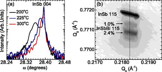
HRXRD scans of InSbBi films on InSb substrates. (a) ω-2θ scans of InSbBi samples grown at temperatures of 200, 225, and 300 °C. (b) Reciprocal space map around the 115 reflection of the InSbBi sample grown at 200 °C.
HRXRD scans of InSbBi films on InSb substrates. (a) ω-2θ scans of InSbBi samples grown at temperatures of 200, 225, and 300 °C. (b) Reciprocal space map around the 115 reflection of the InSbBi sample grown at 200 °C.
The XRD results are consistent with the RBS results. For the sample grown at 200 °C, the 004 peak at ∼28.36° corresponds to the layer with 2.4% Bi and the intensity between that peak and the substrate peak corresponds to the layer containing 1.0% Bi. Intensity associated with these two layers is also apparent in the RSM in Fig. 4(b). The XRD peak for the sample grown at 225 °C corresponds to a Bi content of ∼1.0% Bi, but is broader than expected for a single layer, consistent with the RBS evidence of two separate layers containing 0.85% and 1.2% Bi. For the samples grown at higher temperatures (250–325 °C), the XRD data have a shoulder on the low angle side of the substrate peak, the width of which correlates with the Bi content indicated by RBS for the bottom layer and for the single layer with uniform Bi content for growth at 350 °C. No clear XRD signals were obtained from the higher Bi content layers, consistent with the low Bi substitutionality, and lower crystallinity indicated by RBS for the middle layers.
The InSbBi lattice constant was calculated by considering the tetragonal distortion of the InSbBi films, using the Poisson ratio and elastic constants of InSb.26,27 The lattice parameters in the inset of Fig. 2(b) show a linear trend in accordance with Vegard's law. If this linear trend is extrapolated to 100% Bi, the lattice parameter corresponding to zinc-blende InBi is 6.626 ± 0.010 Å. This is smaller than the 7.292 Å (Ref. 28) and 7.024 Å (Ref. 29) from extrapolating InPBi and InAsBi lattice parameters, respectively, and smaller than the theoretically predicted zinc-blende InBi lattice constant (at 0 K) of 6.686 Å (Ref. 20), but in agreement with the value extrapolated from bulk grown InSbBi samples of 6.638 ± 0.011 Å (from our linear fitting of the data in Ref. 14).
The optical properties of the InSbBi samples as a function of Bi content were studied using transmittance measurements. The transmission data from each sample were divided by the transmission from an InSb substrate so that the remaining signal corresponds to the InSbBi epilayer. The derived absorption spectra are shown in Fig. 5. The inset of Fig. 5 shows the measured absorption edge energy as a function of Bi content. The optical band gap red shifts with increasing Bi content. The sample grown at 200 °C shows two absorption edges corresponding to the layers with Bi content of 1.0% and 2.4%. The absorption between the two extrapolations can be accounted for by the ∼60 nm of the film in which the Bi content changes from 1.0% to 2.4%. When the Bi content is increased to x = 0.024, the absorption edge decreases in energy to ∼88 meV, corresponding to a wavelength of 14.1 μm. The dashed line in the inset of Fig. 5 shows the band gap reduction corresponding to the virtual crystal approximation (VCA). The VCA band gap reduction was calculated using the “negative band gap” of semi-metallic zinc-blende InBi of −1.7 eV from density functional theory,20 which is 19.1 meV/%Bi consisting of 18.8 meV/%Bi lowering of the conduction band minimum (CBM) and 0.3 meV/%Bi increase of the valence band maximum (VBM). The experimentally observed band gap reduction (35 meV/%Bi) exceeds the theoretical prediction of the VCA.

The absorption spectra for InSb1−xBix films. The composition of each film is given in the figure. Where the film comprises multiple layers, these maybe associated with different absorption edges, as indicated. The inset shows the optical band gap versus Bi content determined from the absorption spectra (open circle). The band gap of InSb1−xBix is calculated assuming the VCA variation of both the CBM and the VBM (dashed line) and by assuming the VCA variation of the CBM and VBAC between the valence bands and the Bi impurity level (solid line).
The absorption spectra for InSb1−xBix films. The composition of each film is given in the figure. Where the film comprises multiple layers, these maybe associated with different absorption edges, as indicated. The inset shows the optical band gap versus Bi content determined from the absorption spectra (open circle). The band gap of InSb1−xBix is calculated assuming the VCA variation of both the CBM and the VBM (dashed line) and by assuming the VCA variation of the CBM and VBAC between the valence bands and the Bi impurity level (solid line).
In order to model the experimental data, the valence band anticrossing (VBAC) approach was used. The observed band gap is well reproduced by the 12 × 12 k⋅p model described by Alberi et al. for GaAsSb and GaAsBi.30 The VBAC interaction is included between localized Bi 6p-like states and the host valence bands. The Bi localized state energy level used is 1.2 eV below the InSb VBM. This value was chosen by considering the reported Bi level of 0.4 eV below the VBM in GaAs30 and that the VBM of GaAs is 0.8 eV below that of InSb,26 assuming that the Bi level is approximately equal in different materials on an absolute energy scale. Using this Bi level energy, the interaction strength required to fit the data is 1.35 eV. If the Bi level was closer to the VBM (for example, a value of 0.18 eV below the VBM of GaAs was calculated using tight binding in Ref. 31), a correspondingly lower value of interaction strength would be required. According to this VBAC modeling, a band gap reduction of 33.9 meV/%Bi is made up of 18.8 meV/%Bi VCA lowering of the CBM and 15.1 meV/%Bi due to the upward shift of the VBM predominantly due to the VBAC interaction. This amount of band gap reduction per %Bi for MBE grown material is very similar to the 30 meV/%Bi previously reported for Czochralski-grown bulk InSbBi alloys.13
In conclusion, InSb1−xBix thin films have been grown by MBE. The Bi incorporation induces lattice dilation, in contrast to some of the previous reports. Extrapolation of the InSbBi lattice parameter to 100% Bi suggests a zinc-blende InBi lattice parameter of 6.626 Å. The optical absorption edge decreases at a rate of ∼35 meV/%Bi from 172 meV (7.2 μm) for InSb to ∼88 meV (14.1 μm) for InSb0.976Bi0.024. This makes InSbBi alloys suitable for sources and detectors operating in the 8–14 μm atmospheric transmission window. Further work is required to achieve InSbBi films with uniform Bi content up to 2.4% by exploring the effects of other MBE growth parameters.
The work at Liverpool and Warwick was supported by the University of Liverpool and the Engineering and Physical Sciences Research Council (EPSRC) under Grant Nos. EP/G004447/2 and EP/H021388/1. RBS measurements performed at Lawrence Berkeley National Lab were supported by the U.S. Department of Energy, Office of Science, Basic Energy Sciences, Materials Sciences and Engineering Division. Barry Karlin and Joe Woicik are thanked for use of the X24a HAXPES end station at the National Institute of Standards and Technology bending magnet beamline X24 at the National Synchrotron Light Source at Brookhaven National Laboratory. The National Synchrotron Light Source is supported by the U.S. Department of Energy, Contract No. DE-AC02-98CH10886. The work at Binghamton was supported by a Grant from State University of New York Research Foundation Collaboration Fund.

