Abstract
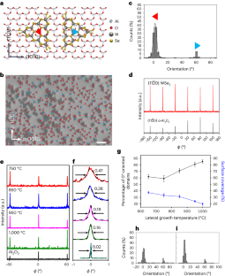
Epitaxial growth of two-dimensional transition metal dichalcogenides on sapphire has emerged as a promising route to wafer-scale single-crystal films. Steps on the sapphire act as sites for transition metal dichalcogenide nucleation and can impart a preferred domain orientation, resulting in a substantial reduction in mirror twins. Here we demonstrate control of both the nucleation site and unidirectional growth direction of WSe2 on c-plane sapphire by metal–organic chemical vapour deposition. The unidirectional orientation is found to be intimately tied to growth conditions via changes in the sapphire surface chemistry that control the step edge location of WSe2 nucleation, imparting either a 0° or 60° orientation relative to the underlying sapphire lattice. The results provide insight into the role of surface chemistry on transition metal dichalcogenide nucleation and domain alignment and demonstrate the ability to engineer domain orientation over wafer-scale substrates.
This is a preview of subscription content, access via your institution
Access options
Access Nature and 54 other Nature Portfolio journals
Get Nature+, our best-value online-access subscription
$29.99 / 30 days
cancel any time
Subscribe to this journal
Receive 12 print issues and online access
$259.00 per year
only $21.58 per issue
Buy this article
- Purchase on Springer Link
- Instant access to full article PDF
Prices may be subject to local taxes which are calculated during checkout


Data availability
Additional data relevant to the conclusions of this study are available in the Supplementary Information. Growth and characterization data associated with the samples produced in this study are available via ScholarSphere52. This includes substrate preparation and recipe data for samples grown by MOCVD in the 2DCC-MIP facility and standard characterization data including AFM images, room-temperature Raman/photoluminescence spectra and field-emission scanning electron microscopy images of the samples. Videos associated with the DFT results are included as Supplementary Videos 1–8 and are available via figshare at https://doi.org/10.6084/m9.figshare.23274647 (ref. 53). Additional datasets related to DFT, SHG, TEM, FET and low-temperature photoluminescence are available from the corresponding author upon request.
References
Acerce, M., Voiry, D. & Chhowalla, M. Metallic 1 T phase MoS2 nanosheets as supercapacitor electrode materials. Nat. Nanotechnol. 10, 313–318 (2015).
Late, D. J., Doneux, T. & Bougouma, M. Single-layer MoSe2 based NH3 gas sensor. Appl. Phys. Lett. 105, 3–7 (2014).
Tan, H. et al. Ultrathin 2D photodetectors utilizing chemical vapor deposition grown WS2 with graphene electrodes. ACS Nano 10, 7866–7873 (2016).
Akinwande, D. et al. Graphene and two-dimensional materials for silicon technology. Nature 573, 507–518 (2019).
Zhou, H. et al. Large area growth and electrical properties of p-type WSe2 atomic layers. Nano Lett. 15, 709–713 (2015).
Terrones, H., López-Urías, F. & Terrones, M. Novel hetero-layered materials with tunable direct band gaps by sandwiching different metal disulfides and diselenides. Sci. Rep. 3, 1–8 (2013).
Yuan, H. et al. Zeeman-type spin splitting controlled by an electric field. Nat. Phys. 9, 563–569 (2013).
Xiao, D. et al. Coupled spin and valley physics in monolayers of MoS2 and other group-VI dichalcogenides. Phys. Rev. Lett. 108, 1–5 (2012).
Fang, H. et al. High-performance single layered WSe2 p-FETs with chemically doped contacts. Nano Lett. 12, 3788–3792 (2012).
Radisavljevic, B., Radenovic, A., Brivio, J., Giacometti, V. & Kis, A. Single-layer MoS2 transistors. Nat. Nanotechnol. 6, 147–150 (2011).
Iqbal, M. W. et al. High-mobility and air-stable single-layer WS2 field-effect transistors sandwiched between chemical vapor deposition-grown hexagonal BN films. Sci. Rep. 5, 10699 (2015).
Chuang, H. J. et al. Highmobility WSe2 p- and n- field-effect transistors contacted by highly doped graphene for low-resistance contacts. Nano Lett. 14, 3594–3601 (2014).
Choudhury, T. H., Zhang, X., Al Balushi, Z. Y., Chubarov, M. & Redwing, J. M. Epitaxial growth of two-dimensional layered transition metal dichalcogenides. Ann. Rev. Mater. Res. 50, 155–177 (2020).
Mortelmans, W., De Gendt, S., Heyns, M. & Merckling, C. Epitaxy of 2D chalcogenides: aspects and consequences of weak van der Waals coupling. Appl. Mater. Today 22, 100975 (2021).
Zhang, X. et al. Diffusion-controlled epitaxy of large area coalesced WSe2 monolayers on sapphire. Nano Lett. 18, 1049–1056 (2018).
Lin, Y. C. et al. Realizing large-scale, electronic-grade two-dimensional semiconductors. ACS Nano 12, 965–975 (2018).
Mortelmans, W. et al. Peculiar alignment and strain of 2D WSe2 grown by van der Waals epitaxy on reconstructed sapphire surfaces. Nanotechnology 30, 465601 (2019).
Dong, J., Zhang, L., Dai, X. & Ding, F. The epitaxy of 2D materials growth. Nat. Commun. 11, 5862 (2020).
Zhou, W. et al. Intrinsic structural defects in monolayer molybdenum disulfide. Nano Lett. 13, 2615–2622 (2013).
Liu, H. et al. Dense network of one-dimensional midgap metallic modes in monolayer MoSe2 and their spatial undulations. Phys. Rev. Lett. 113, 1–5 (2014).
Zou, X., Liu, Y. & Yakobson, B. I. Predicting dislocations and grain boundaries in two-dimensional metal-disulfides from the first principles. Nano Lett. 13, 253–258 (2013).
Du, L. et al. The effect of twin grain boundary tuned by temperature on the electrical transport properties of monolayer MoS2. Crystals 6, 1–9 (2016).
Zhou, S. et al. Atomically sharp interlayer stacking shifts at anti-phase grain boundaries in overlapping MoS2 secondary layers. Nanoscale 10, 16692–16702 (2018).
Chen, L. et al. Step-edge-guided nucleation and growth of aligned WSe2 on sapphire via a layer-over-layer growth mode. ACS Nano 9, 8368–8375 (2015).
Chubarov, M. et al. Wafer-scale epitaxial growth of unidirectional WS2 monolayers on sapphire. ACS Nano 15, 2532–2541 (2021).
Li, T. et al. Epitaxial growth of wafer-scale molybdenum disulfide semiconductor single crystals on sapphire. Nat. Nanotechnol. 16, 1201–1207 (2021).
Hwang, Y. & Shin, N. Hydrogen assisted step-edge nucleation of MoSe2 monolayers on sapphire substrates. Nanoscale 11, 7701–7709 (2019).
Suenaga, K. et al. Surface-mediated aligned growth of monolayer MoS2 and in-plane heterostructures with graphene on sapphire. ACS Nano 12, 10032–10044 (2018).
Cohen, A. et al. Tunsten oxide mediated quasi-van der Waals epitaxy of WS2 on sapphire. ACS Nano 17, 5399–5411 (2023).
Chubarov, M., Choudhury, T. H., Zhang, X. & Redwing, J. M. In-plane X-ray diffraction for characterization of monolayer and few-layer transition metal dichalcogenide films. Nanotechnology 29, 055706 (2018).
Zheng, P. et al. Universal epitaxy of non-centrosymmetric two-dimensional single-crystal metal dichalcogenides. Nat. Comm. 14, 592 (2023).
Tsuda, M. et al. Mechanism of H2 pre-annealing on the growth of GaN on sapphire by MOVPE. Appl. Surf. Sci. 216, 585–589 (2003).
Aljarb, A. et al. Substrate lattice-guided seed formation controls the orientation of 2D transition-metal dichalcogenides. ACS Nano 11, 9215–9222 (2017).
Wang, Y. et al. P-type electrical contacts for 2D transition-metal dichalcogenides. Nature 610, 61–66 (2022).
Wang, Y. et al. Van der Waals contacts between three-dimensional metals and two-dimensional semiconductors. Nature 568, 70–74 (2019).
Garcia, A. et al. Analysis of electron beam damage of exfoliated MoS2 sheets and quantitative HAADF-STEM imaging. Ultramicroscopy 146, 33–38 (2014).
Childres, I. et al. Effect of electron-beam irradiation on graphene field effect devices. Appl. Phys. Lett. 97, 173109 (2010).
Reifsnyder Hickey, D. et al. Illuminating invisible grain boundaries in coalesced single-orientation WS2 monolayer films. Nano Lett. 21, 6487–6495 (2021).
Huang, P. Y. et al. Grains and grain boundaries in single-layer graphene atomic patchwork quilts. Nature 469, 389–392 (2011).
Zeng, H., Dai, J., Yao, W., Xiao, D. & Cui, X. Valley polarization in MoS2 monolayers by optical pumping. Nat. Nanotechnol. 7, 490–493 (2012).
Kim, J. et al. Ultrafast generation of pseudo-magnetic field for valley excitons in WSe2 monolayers. Science 346, 1205–1208 (2014).
Yan, T., Qiao, X., Tan, P. & Zhang, X. Valley depolarization in monolayer WSe2. Sci. Rep. 5, 15625 (2015).
Zhu, B., Zeng, H., Dai, J., Gong, Z. & Cui, X. Anomalously robust valley polarization and valley coherence in bilayer WS2. Proc. Natl Acad. Sci. USA 111, 11606 (2014).
Wang, J. et al. Dual-coupling-guided epitaxial growth of wafer-scale single-crystal WS2 monolayer on vicinal a-plane sapphire. Nat. Nanotechnol. 17, 33–38 (2022).
Kresse, G. & Furthmüller, J. Efficiency of ab-initio total energy calculations for metals and semiconductors using a plane-wave basis set. Comput. Mater. Sci. 6, 15–50 (1996).
Kresse, G. & Furthmüller, J. Efficient iterative schemes for ab initio total-energy calculations using a plane-wave basis set. Phys. Rev. B 54, 11169–11186 (1996).
Kresse, G. & Hafner, J. Ab initio molecular dynamics for liquid metals. Phys. Rev. B 47, 558–561 (1993).
Perdew, J. P., Burke, K. & Ernzerhof, M. Generalized gradient approximation made simple. Phys. Rev. Lett. 77, 3865–3868 (1996).
Perdew, J. P., Burke, K. & Ernzerhof, M. Generalized gradient approximation made simple. Phys. Rev. Lett. 77, 3865–3868 (1996); erratum 78, 1396 (1997).
Kresse, G. & Joubert, D. From ultrasoft pseudopotentials to the projector augmented-wave method. Phys. Rev. B 59, 1758–1775 (1999).
Kresse, G. & Hafner, J. Norm-conserving and ultrasoft pseudopotentials for first-row and transition elements. J. Phys. Condens. Matter 6, 8245–8825 (1994).
Redwing, J. et al. WSe2 on c-plane sapphire with preferred orientation grown by MOCVD. ScholarSphere https://doi.org/10.26207/f7b1-fs46 (2023).
Nayir, N. & van Duin, A. C. T. Movies showing the nucleation of WSe2 on Al2O3 with mixed (Se/O) and single (Se) steps. figshare https://doi.org/10.6084/m9.figshare.23274647 (2023).
Acknowledgements
The work was financially supported by the National Science Foundation (NSF) through the Pennsylvania State University 2D Crystal Consortium–Materials Innovation Platform (2DCC-MIP) under NSF cooperative agreement numbers DMR-1539916 and DMR-2039351. S.B. and N.A. acknowledge support provided by NSF Career grant number DMR-1654107. T.V.M. and J.M.R. acknowledge support from the Defense Technical Information Center under award number FA9550-21-1-0460. N.T. acknowledges support from the NSF Graduate Research Fellowship Program under grant number DGE1255832. K.Z. and S.H. acknowledge support from NSF under grant numbers ECCS-1943895 and ECCS-2246564 and Air Force Office of Scientific Research under grant number FA9550-22-1-0408. SHG measurements were supported by the Center for Nanophase Materials Sciences (CNMS), which is a US Department of Energy Office of Science User Facility at Oak Ridge National Laboratory.
Author information
Authors and Affiliations
Contributions
H.Z. and T.H.C. carried out MOCVD growth, AFM, field-emission scanning electron microscopy and in-plane XRD characterization and data analysis with assistance from K.Y., T.V.M.K., N.T., R.A.M. and S.M.D. N.N., V.H.C. and A.C.T.v.D. carried out DFT calculations. A.B. and B.H. performed in-plane XRD, layer transfer and Raman/photoluminescence characterizations. K.Z. and S.H. performed low-temperature and polarization-resolved photoluminescence measurements. A.A.P. performed SHG characterization. S.B., N.A. and K.W. performed transmission electron microscopy characterizations. A.O. and S.D. fabricated and tested backgated FETs. H.Z., N.N., T.H.C. and J.M.R. co-wrote the manuscript with input from all authors. All authors contributed to the discussions.
Corresponding author
Ethics declarations
Competing interests
The authors declare no competing interests.
Peer review
Peer review information
Nature Nanotechnology thanks Wouter Mortelmans and the other, anonymous, reviewer(s) for their contribution to the peer review of this work.
Additional information
Publisher’s note Springer Nature remains neutral with regard to jurisdictional claims in published maps and institutional affiliations.
Supplementary information
Supplementary Information
Supplementary Figs. 1–26 and Discussion.
Supplementary Video 1
Nucleation of a TRIANGULAR WSe2 on the BOTTOM terrace of a MIXED Se/O step.
Supplementary Video 2
Nucleation of a TRIANGULAR WSe2 on the TOP terrace of a MIXED Se/O step.
Supplementary Video 3
Nucleation of a TRIANGULAR WSe2 on the BOTTOM terrace of a SINGLE Se step.
Supplementary Video 4
Nucleation of a TRIANGULAR WSe2 on the TOP terrace of a SINGLE Se step.
Supplementary Video 5
Nucleation of a RIBBON WSe2 on the BOTTOM terrace of a MIXED Se/O step.
Supplementary Video 6
Nucleation of a RIBBON WSe2 on the TOP terrace of a MIXED Se/O step.
Supplementary Video 7
Nucleation of a RIBBON WSe2 on the BOTTOM terrace of a SINGLE Se step.
Supplementary Video 8
Nucleation of a RIBBON WSe2 on the TOP terrace of a SINGLE Se step.
Rights and permissions
Springer Nature or its licensor (e.g. a society or other partner) holds exclusive rights to this article under a publishing agreement with the author(s) or other rightsholder(s); author self-archiving of the accepted manuscript version of this article is solely governed by the terms of such publishing agreement and applicable law.
About this article
Cite this article
Zhu, H., Nayir, N., Choudhury, T.H. et al. Step engineering for nucleation and domain orientation control in WSe2 epitaxy on c-plane sapphire. Nat. Nanotechnol. 18, 1295–1302 (2023). https://doi.org/10.1038/s41565-023-01456-6
Received:
Accepted:
Published:
Issue Date:
DOI: https://doi.org/10.1038/s41565-023-01456-6
This article is cited by
-
3D integration of 2D electronics
Nature Reviews Electrical Engineering (2024)
-
Three-dimensional integration of two-dimensional field-effect transistors
Nature (2024)
-
Epitaxy of wafer-scale single-crystal MoS2 monolayer via buffer layer control
Nature Communications (2024)
-
Vapour-phase deposition of two-dimensional layered chalcogenides
Nature Reviews Materials (2023)
-
p-Type Two-Dimensional Semiconductors: From Materials Preparation to Electronic Applications
Nano-Micro Letters (2023)


