
Abstract
Electro-absorption (EA) waveguide-coupled modulators are essential building blocks for on-chip optical communications. Compared to state-of-the-art silicon (Si) devices, graphene-based EA modulators promise smaller footprints, larger temperature stability, cost-effective integration and high speeds. However, combining high speed and large modulation efficiencies in a single graphene-based device has remained elusive so far. In this work, we overcome this fundamental trade-off by demonstrating the 2D-3D dielectric integration in a high-quality encapsulated graphene device. We integrated hafnium oxide (HfO2) and two-dimensional hexagonal boron nitride (hBN) within the insulating section of a double-layer (DL) graphene EA modulator. This combination of materials allows for a high-quality modulator device with high performances: a ~39 GHz bandwidth (BW) with a three-fold increase in modulation efficiency compared to previously reported high-speed modulators. This 2D-3D dielectric integration paves the way to a plethora of electronic and opto-electronic devices with enhanced performance and stability, while expanding the freedom for new device designs.
Introduction
Broadband optical modulators with ultra-high-speed, low-drive voltage, and hysteresis-free operation are key devices for next-generation datacom transceivers1. Although Si photonics is nowadays a prime candidate to fulfill these requirements2,3, graphene is rapidly becoming a major contender in several optoelectronic applications, such as ultrafast modulators4,5 and silicon-integrated photodetectors6,7. Graphene-based modulators have already proven broadband optical bandwidth1, high speed8,9, relatively high modulation efficiencies10, and temperature stability8. These devices are all based on complementary metal–oxide–semiconductor (CMOS)-compatible material7,10,11,12,13, where CMOS design and fabrication techniques can be further leveraged to decrease costs. However, graphene-based modulators are yet to demonstrate all operation requirements at once. More specifically, EA graphene modulators struggle to show high-speed and high modulation efficiencies simultaneously14. This bottleneck is mostly due to the weak graphene/dielectric combination and the limited quality of graphene.
Unlike Si technology, where high-κ dielectrics lie at the core of its success, 2D dielectrics are hindering the development of graphene- and other 2D-based electronics and optoelectronic devices1,13,15 and are clearly outperformed by traditional 3D high-κ dielectrics. This underperforming 2D-dielectric/graphene combination deepens even further the fundamental trade-off between speed and modulation efficiency inherent to the double-layer (DL) modulators14. In the DL architecture, the overlapped top and bottom graphene electrodes act as a capacitor (C). The larger the C, the higher the modulation efficiency. On the other hand, the speed of the modulator defined as f3dB = 1/(2πRC) is inversely proportional to C (R being the total resistance). In this framework, the quality of graphene appears as a valid turnaround to overcome this fundamental limitation. High electron mobility is expected to minimize the overall resistance and reduce the insertion loss (IL)1,9, thus increasing the bandwidth and the extinction ratio (ER). However, the quality of graphene is very sensitive to its environment, e.g., the dielectric to encapsulate it. Indeed, no graphene/dielectric combination has been able to ensure high charge carrier mobilities and low levels of residual doping in existing graphene waveguide-coupled modulators16. The growth of nonlayered (i.e., 3D) dielectrics, e.g., aluminum oxide (Al2O3), silicon nitride (\({\rm{SiN}}\)), or HfO2 directly on top of graphene leads to low electronic mobility16,17,18 and/or inhomogeneous doping19.
In this work, we demonstrate the 2D–3D integration of hBN and HfO2 within the dielectric section of a DL graphene EA modulator. This dielectric combination enhances the capacitance of the EA modulators without compromising their robustness against high voltages and preserves the high mobility and low doping of intrinsic graphene. As a result, we achieved a static and dynamic (at 40 Gbps) modulation efficiency as high as 2.2 and 1.49 dBV−1, respectively, a f3dB bandwidth of ~39 GHz, and a device footprint of 60 μm × 0.45 μm ≈ 27 μm2 (neglecting the metal pads and graphene leads). Moreover, the hBN–HfO2–hBN-based devices show a symmetric and nearly hysteresis-free operation. The larger breakdown voltage of this 2D–3D dielectric, even beyond the full transparency regime (i.e., Pauli blocking), increases the ER and reduces the IL of the modulators.
Results
The EA modulators were fabricated on top of a photonic structure20 formed by two grating couplers21 feeding light in and out of an optical waveguide (Fig. 1a). The 750-nm-wide waveguide for the device in Fig. 1 was designed to support a single transverse–magnetic (TM) optical mode20 (see Supplementary Note 3). The presented DL graphene modulators were built, with hBN-encapsulated graphene top and bottom electrodes (Fig. 1d). The hBN–graphene–hBN stacks have been fabricated following state-of-the-art fabrication techniques22,23. This ensured low levels of doping and high charge carrier mobilities. We characterized the quality of the resulting modulators (see Supplementary Notes 2 and 6) and extracted a carrier density-independent mobility as high as 30,000 cm2 V−1 s−1 at room temperature23 (see Supplementary Note 2).
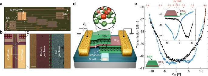
a Optical image of a photonic device consisting of two grating couplers (GC), a silicon optical waveguide (Si WG), and an hBN–HfO2–hBN-based graphene EA modulator on top (see zoom-in optical (panel b) and scanning electron microscope (SEM) (panel c) images for details). In panel c, the metal contacts are yellow/brown and the bottom and top graphene electrodes violet and light blue, respectively. The core of the waveguide is highlighted by the green dashed lines. The white scale bars in panel a, b, and c are 100, 5, and 1 μm, respectively. d Electrical connections and schematic cross-section of an EA modulator with an hBN–HfO2–hBN dielectric. The top and bottom graphene electrodes are fully encapsulated by hBN (in green) protecting both graphene electrodes from the out-of-plane dangling bonds typical of 3D oxide materials, e.g., HfO2 (in red). See inset for a molecular representation. e Transmission curves as a function of the voltage between the bottom and top graphene electrodes (VBT axis, bottom) and the Fermi energy at the graphene electrodes (EF axis, top) for the EA modulator in panel a with an hBN–HfO2–hBN dielectric (see sketch). The 1550 nm excitation power was set to 0 dBm. The forward and backward voltage sweeps (black and blue, respectively) show no major hysteresis compared to a modulator with an hBN–HfO2 dielectric (see inset). The red line is a linear fit to the forward voltage sweep within a 0.5 V voltage span (extracted slope: 2.2 dBV−1).
Although hBN-encapsulated graphene devices have allowed for device designs with unprecedented functionalities24,25,26 and improved performance23, such layered dielectric material typically contains impurities and/or crystal defects leading to low breakdown voltages27,28. Moreover, the dielectric permittivity of hBN is rather low compared to existing high-κ dielectrics29, with a value close to that of SiO2 (ϵr ~ 4). This low dielectric constant and reduced breakdown voltage (see Supplementary Note 5) compromises not only the power consumption and the ability to reach high modulation efficiencies at reasonably low drive voltages but also limits the IL and the ER of the modulators1,9. We thus integrate HfO2, a high-κ dielectric material, within the hBN-encapsulated graphene electrodes (see the sketch in Fig. 1d).
With such hBN–HfO2–hBN dielectric arrangement, graphene remains isolated from HfO2, shielded away from any possible out-of-plane dangling bonds of the 3D oxide material (see inset of Fig. 1d for the molecular representation of the 2D–3D dielectric interface). More importantly, the hBN–graphene interfaces remain atomically sharp and clean22,23,30. This nanoscale control of the interfaces brings further advantages to real-world EA graphene modulators, like a symmetric and hysteresis-free operation. This is directly visible in the transmission curves as a function of the applied voltage VBT or, alternatively, as a function of the Fermi energy EF at the graphene electrodes (see the bottom and top axis in Fig. 1e and Supplementary Note 9). Both forward and backward voltage sweeps (black and blue traces, respectively) show minor hysteresis and appear symmetric with respect to the charge neutrality point. For comparison, a device fabricated with a HfO2–hBN dielectric shows no overlap between the forward and backward sweeps (inset of Fig. 1e). This strong hysteresis is nonetheless expected for this HfO2–hBN modulator since, in that case, the top graphene electrode is in direct contact with HfO2. The hBN–HfO2–hBN modulator device exhibits a modulation efficiency as high as ~2.2 dBV−1 within a 0.5 V voltage span (see red linear fit to the data in Fig. 1e). Considering the length of our modulator (~60 μm), we obtain a normalized static modulation efficiency of ~0.037 dBV−1 μm−1, a threefold increase compared to previously reported high-speed graphene EA modulators9.
With such a high static modulation efficiency (Fig. 1), one might expect the device speed to be compromised14. However, the high mobility of the hBN-encapsulated graphene is expected to increase the bandwidth. This is visible in Fig. 2a, where we calculated the f3dB bandwidth as a function of the charge carrier-dependent mobility (μ) and contact resistivity (ρc) for a graphene modulator with the same geometry and dielectric combination as the device in Fig. 1 (see Supplementary Note 11). As observed, the graphene mobility and the contact resistivity have a major influence on the modulator speed. Considering the mobility μ ≈ 12,000 cm2 V−1 s−1 (evaluated at VBT = 10.4 V) and the contact resistivity ρc ≈ 800 Ω μm achieved experimentally (see Supplementary Notes 4 and 11), we expect a bandwidth of f3dB ~ 46 GHz (dashed lines in Fig. 2a). To confirm this value experimentally, we measured the electro-optical (EO) bandwidth of the device in Fig. 1 at a DC voltage VBT = 10.4 V and a peak-to-peak voltage VAC = 200 mV (Fig. 2b). The bandwidth of the measured device attains f3dB ≈ 39 GHz (without de-embedding, see Supplementary Note 13). This value is close to the capabilities of our setup, limited to 40 GHz by the vector network analyzer and the RF probes (see Supplementary Note 12). Even though the measured f3dB does not reach the expected f3dB ~ 46 GHz (Fig. 2a), possibly due to an increased contact resistivity of the measuring device (see Supplementary Note 11), this is still the highest f3dB bandwidth among all graphene-based modulators reported so far8,9,11,12,31,32.

a f3dB bandwidth as a function of the charge carrier-dependent mobility (μ) and the contact resistivity (ρc) calculated for a device with the same geometry and dielectric combination as the device in Fig. 1 (see Supplementary Note 11). The dashed lines indicate the expected f3dB ~46 GHz at μ ~12,000 cm2 V−1 s−1 (evaluated at VBT = 10.4 V, refer to panel b). b Measured electro-optical S21 frequency response of the EA modulator at VBT = 10.4 V and VAC = 200 mV, without de-embedding, i.e., including the contributions of the setup and photodetector (see Supplementary Note 12). c In all, 231 − 1 pseudo-random binary sequence non-return-to-zero eye diagram at 28 and 40 Gbps. The EA modulator is d.c. biased at VBT = 11 V and driven by a VAC = 3.5 V peak-to-peak RF signal. The eye diagram measured at 40 Gbps has a 5.2 dB ER and a 2.28 dB signal-to-noise ratio (SNR). The green arrows indicate the 0 W baseline, and the white scale bar corresponds to 10 ps.
The high-speed operation of our modulator device is also supported by non-return-to-zero eye diagram measurements. The data were obtained through an electrical pattern generator (PG) driving the modulator with a 231 − 1 pseudo-random binary sequence at 28 and 40 Gbps bit-rate (see Supplementary Note 13). The signal was driven by a 3.5-V peak-to-peak voltage while the DC bias was set to 11 V. The device was terminated with a 50 Ω load to avoid reflections due to the impedance mismatch between the PG electrical output and the modulator (when measured at 40 Gbps). Open eye diagrams at 28 and 40 Gbps are shown in Fig. 2c, with an ER as high as 5.2 dB and a signal-to-noise ratio of 2.28 dB for the latter (see Supplementary Note 14 for an eye diagram at 10 Gbps). These results confirm the large modulation efficiency of our hBN–HfO2–hBN-based modulator device, even at high speeds, with a dynamic modulation efficiency of 1.49 dBV−1 at 40 Gbps9.
Like the speed of the modulator, the power consumption understood as the switching energy per bit also benefits from the small footprint of the device. Ignoring the parasitic pad capacitance, we obtain for the modulator in Fig. 1 an energy per bit of \(C{({V}_{{\rm{AC}}})}^{2}/4\approx {160}\ {{\rm{fJbit}}}^{-1}\), where C = 52 fF is the capacitance between the top and bottom graphene electrodes and VAC = 3.5 V the voltage swing12. This value of energy per bit is on par with state-of-the-art SiGe technologies33,34.
To directly compare modulators with different dielectrics, it is more convenient to compare the transmission as a function of EF (see the EF axis in Figs. 1e and 3b and c) since EF already considers the thickness and the relative permittivity of the dielectric (see Supplementary Note 7). Operating the modulators at high EF enhances both ER and IL, with the ER (IL) increasing (decreasing) as a function of EF9. In the full transparency regime (Pauli blocking, see Supplementary Note 1), the ER is maximized and the IL is expected to become nearly zero for high-quality graphene1,9 (see Supplementary Note 10). It is thus crucial to determine which dielectric materials facilitate Pauli blocking operation. Figure 3a illustrates the expected maximum EF,
as a function of the relative permittivity (ϵr) and dielectric strength (EBD) of any given dielectric. The square boxes in Fig. 3a enclose the expected \({E}_{{\rm{F}}}^{\max }\) for the HfO2− and hBN-based modulators (in red and green, respectively) and the black star represents the \({E}_{{\rm{F}}}^{\max }=0.57\) eV expected for the hBN–HfO2–hBN modulator of Fig. 1e (see Supplementary Note 10). The boundaries of the boxes are taken from literature28,35,36,37 (marked with dots) and from our dielectric characterization (marked with stars, see Supplementary Notes 5 and 10). All dielectric materials fulfilling \({E}_{{\rm{F}}}^{\max }\,> \, 0.5\) eV (see white fringe in Fig. 3a) allow full transparency, i.e., Pauli blocking. The comparison in Fig. 3a highlights the advantages of the hBN–HfO2–hBN dielectric (black star), achieving higher EF values than the hBN dielectric while equally preserving the intrinsic qualities of graphene.

a Maximum Fermi energy, noted \({E}_{{\rm{F}}}^{\max }\), expected at the graphene electrodes of a graphene modulator with a dielectric’s relative permittivity ϵr and dielectric strength EBD. All points lying inside the blue-colored region represent a dielectric allowing for Pauli blocking operation (\({E}_{{\rm{F}}}^{\max }\,> \, 0.5\) eV, refer to Supplementary Note 1). The red-colored region indicates otherwise (\({E}_{{\rm{F}}}^{\max }\,<\, 0.5\) eV). The white band represents the Pauli blocking boundary condition, defined as \({E}_{{\rm{F}}}^{\max }=0.5\) eV. The expected \({E}_{{\rm{F}}}^{\max }\) for HfO2 and hBN are represented by the red and green squares, respectively, taking the values of EBD and ϵr from literature28,35,36,37 (marked with dots) and our dielectric characterization (marked with stars, see Supplementary Notes 5 and 10). The black star represents the \({E}_{{\rm{F}}}^{\max }=0.57\) eV expected for the hBN–HfO2–hBN modulator in Fig. 1e (see Supplementary Note 10). b, c Normalized transmission as a function of EF and VBT for modulators with hBN (b) and hBN–HfO2–hBN (c) dielectric. The data points are measurements and the solid curves simulations (see Supplementary Notes 1–3 and 10). The vertical dashed lines indicate the \({E}_{{\rm{F}}}^{\max }\) achieved at the dielectric breakdown. The orange-shaded regions show the full transparency range, i.e., Pauli blocking. The top VBT axis in panel b is for the 42 μm-long device only (see Supplementary Note 7 for the other hBN devices). The graphene Dirac cones in panel b show the absorption and Pauli blocking processes at low and high Fermi energies, respectively.
These results are confirmed by the transmission traces in Fig. 3b, c. None of the hBN-based modulators were able to withstand Pauli blocking operation (orange-shaded region Fig. 3b), all breaking their hBN dielectric at a similar \({E}_{{\rm{F}}}^{\max }\approx 0.4\) eV (see vertical dashed lines in Fig. 3b and Supplementary Notes 7 and 8). Even though these hBN-based modulators were too fragile, we obtained modulation efficiencies as high as 0.3, 1.3, and 2 dBV−1 for device lengths L = 12, 24, and 42 μm, respectively. Once normalized by its length, we obtain 0.025, 0.054, and 0.047 dBV−1 μm−1. These results exceed the state-of-the-art modulation efficiency of 0.038 dBV−1 μm−110. Still, the premature hBN breakdown compromises the ER and the IL. Indeed, the measured ER = 0.75, 2.3, and 4.9 dB (data points in Fig. 3b) is far from the simulated ER = 1.8, 4.4, and 7.9 dB (solid traces in Fig. 3b) expected for the 12, 24, and 42 μm-long modulators, respectively (for simulations, refer to Supplementary Notes 1–3). Likewise, the measured IL = 1, 2.2, and 3.4 dB are higher than IL ≈0 dB expected for high-mobility graphene modulators1 (see the minimum 0-dB normalized transmission, i.e., neglecting the losses from grating couplers and Si waveguide, achieved by the simulation traces in Fig. 3b and Supplementary Note 10).
On the other hand, the second hBN–HfO2–hBN modulator device attains the Pauli blocking regime (Fig. 3c), in agreement with the dielectric characterization of hBN–HfO2–hBN (Fig. 3a and Supplementary Notes 5 and 10), reaching a maximum Fermi energy of \({E}_{{\rm{F}}}^{\max }\approx 0.54\) eV. The ER and IL improve accordingly, with an ER = 7.8 dB almost twice the value obtained by the hBN-based modulator of comparable length (compare the black and red traces of Fig. 3c, b, respectively) and an IL reaching nearly zero (IL ≈ 0.04 dB in Fig. 3c and Supplementary Note 10). However, being shorter (L = 44 μm) than the device in Fig. 1e (L = 60 μm), the modulation efficiency is lower (1.3 dBV−1 in a 0.5 V span, see Fig. 3c). We note that the hBN–HfO2–hBN device of Fig. 1e has a relatively weak measured ER ≈ 4.4 dB and IL ≈7.8 dB (see Supplementary Note 10) due to an overcautious VBT = 12.1 V applied voltage (or alternatively EF = 0.41 eV). Considering the breakdown capabilities of hBN–HfO2–hBN dielectric (black star in Fig. 3a), we evaluated a potential ER ≈ 12 dB and IL ≈ 0.042 dB for this device (see Supplementary Note 10).
Discussion
Although material platforms like lithium niobate38 (LiNbO3) or hybrid technologies like Si/indium phosphide39 (InP), Si/SiGe40, or InGaAlAs40 offer outstanding performances in modulator applications, those are either not scalable38,41 (LiNbO3) or their integration with a CMOS fabrication line remains challenging40,42. Nowadays, Si and graphene are envisaged as the most scalable, cost-effective, and CMOS-compatible materials for amplitude modulator applications1. To compare our results with state-of-the-art graphene and Si amplitude modulators, both EA and Mach–Zehnder interferometer configurations included, we summarize our results in Fig. 4 and in Supplementary Notes 15 and 16. Figure 4 shows the dynamic modulation efficiency (extracted from the eye diagrams and normalized by the device length and drive voltage) as a function of the modulation speed (red axis and red data point in Fig. 4) and the static modulation efficiency (measured in DC and normalized by the device length), as a function of the f3dB bandwidth (black axis and black data point in Fig. 4). To avoid discrepancies due to the different extraction methods, we determine the static modulation efficiency of the compared literature8,9,10,11,12 using the same method as in Fig. 1e, i.e., by applying a linear fit within a 0.5 V voltage span. The results highlight the trade-offs between speed and modulation efficiency and stress the advantages of an hBN–HfO2–hBN dielectric to obtain large static and dynamic modulation efficiencies even at high speed. As observed, the modulation efficiency typically drops for devices with high speed8,9, being our device the only modulator able to operate at high speed with a large static and dynamic modulation efficiency (Fig. 4). These results outperform state-of-the-art graphene and not-yet-commercial silicon-based electroabsorption modulators43,44,45 (see blue/red and green data clouds, respectively in Fig. 4) when considering the modulation efficiency normalized by the length (i.e., footprint). This figure-of-merit is rather an important one since for many envisaged applications (e.g., chip interconnects), multiple modulator devices are expected to coexist on the same chip.

The black and red data points and axis represent the static modulation efficiency as a function of the f3dB bandwidth and the dynamic modulation efficiency (extracted from eye diagrams) as a function of the modulation speed, respectively. The red, blue, and green data clouds enclose single-11,12,31,46 and double-layer8,9,10,32 graphene and silicon43,44,45 state-of-the-art modulators operating at λ = 1.55 μm. Refer to Supplementary Notes 15 and 16 for a more detailed comparison of graphene-based modulators.
In this work, we demonstrated the advantages of integrating hBN with a 3D high-κ dielectric for high-quality graphene-based EA modulators. Compared to traditional oxide sputtering or atomic layer deposition (ALD) growth on top of graphene, the integration of HfO2 in-between hBN prevented any damage to the underlying graphene and allowed clean graphene–hBN interfaces. These clean interfaces yielded a symmetric and nearly hysteresis-free operation. Moreover, this 2D–3D integration enabled full transparency while maintaining the high mobility and low doping of intrinsic graphene. More importantly, the hBN–HfO2–hBN-based EA modulators were able to reach high modulation speeds with strong modulation efficiencies, overcoming the fundamental limitations of the DL graphene configuration and outperforming state-of-the-art graphene and Si technologies. The compatibility of this hBN–HfO2–hBN dielectric with Si and other 2D materials might allow for considerable scaling improvements and greater device functionality in a broad range of graphene- and 2D-based electronic and optoelectronic applications, even beyond graphene-based modulators.
Methods
Device fabrication
The Si photonic waveguide with a core cross-section of 750 nm × 220 nm was prepared on the IMEC iSiPP25G silicon-on-insulator platform20. For the fabrication of the electroabsorption modulator, the graphene and hBN flakes were exfoliated from highly oriented pyrolytic graphite and hBN crystals, respectively. The bottom hBN–graphene–hBN stacks were prepared by the van der Waals assembly technique22,23 and transferred directly onto the Si waveguide separated by a 10 nm spacer of high-quality thermal SiO2. The bottom hBN flake (separating the graphene and the SiO2 layer) thickness of ~5 nm was chosen to enhance the graphene absorption while isolating the graphene from the rough SiO2 substrate. The top hBN has a thickness of ~10 nm. The stack has been etched by reactive ion etching in an oxygen (O2) and trifluoromethane (CHF3) (4:40 sccm) environment to expose the graphene edge. The bottom stack was then contacted by a 3/15/30 nm Cr/Pd/Au metal combination. The 10 nm hafnium oxide film has been deposited at 250 °C prior depositions of a 2 nm sputtered SiO2 seed layer by ALD. Tetrakis-dimethylamido hafnium (TDMAH) (0.4 s purge time) and water vapor (5 s purge time) as precursors have been used in a Savannah G1 system from Cambridge Nanotech. The top hBN–graphene–hBN stack with a 7 nm- and 21 nm-thick bottom and top hBN layers has followed the same fabrication steps as the bottom stack.
Data availability
The data that support the plots within this paper and other findings of this study are available from the corresponding author upon reasonable request.
References
Romagnoli, M. et al. Graphene-based integrated photonics for next-generation datacom and telecom. Nat. Rev. Mater. 3, 392 (2018).
Chaisakul, P. et al. Recent progress on Ge/SiGe quantum well optical modulators, detectors, and emitters for optical interconnects. Photonics 6, 24 (2019).
Reed, G. T., Mashanovich, G., Gardes, F. Y. & Thomson, D. J. Silicon optical modulators. Nat. Photonics 4, 518–526 (2010).
Luo, S., Wang, Y., Tong, X. & Wang, Z. Graphene-based optical modulators. Nanosc. Res. Lett. 10, 199 (2015).
Shu, H., Jin, M. & Tao, Y. Graphene-based silicon modulators. Front. Inf. Technol. Electron. Eng. 20, 458–471 (2019).
Goossens, S. et al. Broadband image sensor array based on graphene-CMOS integration. Nat. Photonics 11, 366–371 (2017).
Akinwande, D. et al. Graphene and two-dimensional materials for silicon technology. Nature 573, 507–518 (2019).
Dalir, H., Xia, Y., Wang, Y. & Zhang, X. Athermal broadband graphene optical modulator with 35 GHz speed. ACS Photonics 3, 1564–1568 (2016).
Giambra, M. A. et al. High-speed double layer graphene electro-absorption modulator on SOI waveguide. Opt. Express 27, 20145–20155 (2019).
Liu, M., Yin, X. & Zhang, X. Double-layer graphene optical modulator. Nano Lett. 12, 1482–1485 (2012).
Liu, M. et al. A graphene-based broadband optical modulator. Nature 474, 64–67 (2011).
Hu, Y. et al. Broadband 10 Gb/s operation of graphene electro-absorption modulator on silicon. Laser & Photonics Rev. 10, 307–316 (2016).
Neumaier, D., Pindl, S. & Lemme, M. C. Integrating graphene into semiconductor fabrication lines. Nat. Mater. 18, 525–529 (2019).
Phare, C. T., Lee, Y.-H. D., Cardenas, J. & Lipson, M. Graphene electro-optic modulator with 30 GHz bandwidth. Nat. Photonics 9, 511–514 (2015).
Li, W. et al. Uniform and ultrathin high-κ gate dielectrics for two-dimensional electronic devices. Nat. Electron. 2, 563–571 (2019).
Zhu, W., Neumayer, D., Perebeinos, V. & Avouris, P. Silicon nitride gate dielectrics and band gap engineering in graphene layers. Nano Lett. 10, 3572–3576 (2010).
Lemme, M. C., Echtermeyer, T. J., Baus, M. & Kurz, H. A graphene field-effect device. IEEE Electron Device Lett. 28, 282–284 (2007).
Zhou, P. et al. Direct deposition of uniform high-κ dielectrics on graphene. Sci. Rep. 4, 6448 (2014).
Alles, H. et al. Atomic layer deposition of high-k oxides on graphene. Graphene-Synthesis, Characterization, Properties and Applications 99–101 (2011).
Absil, P. P. et al. Imec iSiPP25G silicon photonics: a robust CMOS-based photonics technology platform. in Silicon Photonics X, vol. 9367, 166–171 (2015).
Roelkens, G., van Thourhout, D. & Baets, R. High efficiency Silicon-on-Insulator grating coupler based on a poly-Silicon overlay. Opt. Express 14, 11622–11630 (2006).
Pizzocchero, F. et al. The hot pick-up technique for batch assembly of van der Waals heterostructures. Nat. Commun. 7, 11894 (2016).
Purdie, D. G. et al. Cleaning interfaces in layered materials heterostructures. Nat. Commun. 9, 5387 (2018).
Kamalakar, M. V., Dankert, A., Bergsten, J., Ive, T. & Dash, S. P. Enhanced tunnel spin injection into graphene using chemical vapor deposited hexagonal boron nitride. Sci. Rep. 4, 6146 (2014).
Britnell, L. et al. Field-effect tunneling transistor based on vertical graphene heterostructures. Science 335, 947–950 (2012).
Terrés, B. et al. Size quantization of Dirac fermions in graphene constrictions. Nat. Commun. 7, 11528 (2016).
Hattori, Y., Taniguchi, T., Watanabe, K. & Nagashio, K. Layer-by-layer dielectric breakdown of hexagonal boron nitride. ACS Nano 9, 916–921 (2015).
Hattori, Y., Taniguchi, T., Watanabe, K. & Nagashio, K. Anisotropic dielectric breakdown strength of single crystal hexagonal boron nitride. ACS Appl. Mater. Interfaces 8, 27877–27884 (2016).
Peimyoo, N. et al. Laser-writable high-κ dielectric for van der Waals nanoelectronics. Sci. Adv. 5.1 (2019).
Fazio, D. D. et al. High-mobility, wet-transferred graphene grown by chemical vapor deposition. ACS Nano 13, 8926–8935 (2019).
Sorianello, V. et al. Chirp management in silicon-graphene electro absorption modulators. Opt. Express 25, 19371–19381 (2017).
Mohsin, M. et al. Graphene based low insertion loss electro-absorption modulator on SOI waveguide. Opt. Express 22, 15292–15297 (2014).
Edwards, E. H. et al. Ge/SiGe asymmetric Fabry-Perot quantum well electroabsorption modulators. Opt. Express 20, 29164–29173 (2012).
Audet, R. M. et al. Surface-normal Ge/SiGe asymmetric Fabry-Perot optical modulators fabricated on silicon substrates. J. Lightw. Technol. 31, 3995–4003 (2013).
Lukosius, M. et al. Atomic-vapour-deposited HfO2 and Sr4 Ta2 O9 layers for metal-insulator-metal applications. Microelectron. Eng. 84, 2165–2168 (2007).
Lin, H. C., Ye, P. D. & Wilk, G. D. Leakage current and breakdown electric-field studies on ultrathin atomic-layer-deposited Al2 O3 on GaAs. Appl. Phys. Lett. 87, 182904 (2005).
Groner, M. D., Elam, J. W., Fabreguette, F. H. & George, S. M. Electrical characterization of thin Al2 O3 films grown by atomic layer deposition on silicon and various metal substrates. Thin Solid Films 413, 186–197 (2002).
Mercante, A. J. et al. Thin film lithium niobate electro-optic modulator with terahertz operating bandwidth. Optics Express 26, 14810–14816 (2018).
Smit, M., Williams, K. & van der Tol, J. Past, present, and future of InP-based photonic integration. APL Photonics 4, 050901 (2019).
Liu, K., Ye, C. R., Khan, S. & Sorger, V. J. Review and perspective on ultrafast wavelength-size electro-optic modulators. Laser Photonics Rev. 9, 172–194 (2015).
Wang, C., Zhang, M., Stern, B., Lipson, M. & Lončar, M. Nanophotonic lithium niobate electro-optic modulators. Opt. Express 26, 1547–1555 (2018).
Tang, Y. et al. 50 Gb/s hybrid silicon traveling-wave electroabsorption modulator. Opt. Express 19, 5811–5816 (2011).
Giewont, K. et al. 300-mm monolithic silicon photonics foundry technology. IEEE J. Select. Top. Quantum Electron. 25, 1–11 (2019).
Gill, D. M. et al. Demonstration of error-free 32-Gb/s operation from monolithic CMOS nanophotonic transmitters. IEEE Photonics Technol. Lett. 28, 1410–1413 (2016).
Xiong, C. et al. Monolithic 56 Gb/s silicon photonic pulse-amplitude modulation transmitter. Optica 3, 1060–1065 (2016).
Sorianello, V. et al. Graphene-silicon phase modulators with gigahertz bandwidth. Nat. Photonics 12, 40–44 (2018).
Acknowledgements
We thank S. Pradhan for his assistance in capacitance measurements and D.A. Iranzo for his inputs on the illustration in Fig. 1d. We also thank T. Khodkov, D.B. Ruiz, and S. Castilla for technical assistance. The research leading to these results has received funding from the European Union’s Horizon 2020 research and innovation program under grant agreement No. 881603 (Graphene flagship Core3). H.A. also acknowledges funding from the European Union’s Horizon 2020 research and innovation program under the Marie Skłodowska-Curie grant agreement No. 665884. F.H.L.K. also acknowledges support from the Government of Spain (FIS2016-81044, Severo Ochoa CEX2019-000910-S), Fundació Cellex, Fundació Mir-Puig, and Generalitat de Catalunya (CERCA, AGAUR, and SGR 1656). K.W. and T.T. acknowledge support from the Elemental Strategy Initiative conducted by the MEXT, Japan, Grant Number JPMXP0112101001, JSPS KAKENHI Grant Number JP20H00354 and the CREST(JPMJCR15F3), JST.
Author information
Authors and Affiliations
Contributions
B.T., H.A., and F.H.L.K. conceived the idea. H.A. and B.T. fabricated the devices. L.O. and B.T. did the simulations. B.T. and H.A. performed the measurements and data analysis. A.M. and V.S. performed high-frequency measurements under the supervision of M.R. M.P. and D.V.T. provided Si waveguides. K.W. and T.T. synthesized the hBN crystals. F.H.L.K. and B.T. supervised the project. B.T., H.A., and F.H.L.K. wrote the paper with input from all authors.
Corresponding authors
Ethics declarations
Competing interests
The authors declare no competing interests.
Additional information
Peer review information Nature Communications thanks the anonymous reviewer(s) for their contribution to the peer review of this work.
Publisher’s note Springer Nature remains neutral with regard to jurisdictional claims in published maps and institutional affiliations.
Supplementary information
Rights and permissions
Open Access This article is licensed under a Creative Commons Attribution 4.0 International License, which permits use, sharing, adaptation, distribution and reproduction in any medium or format, as long as you give appropriate credit to the original author(s) and the source, provide a link to the Creative Commons license, and indicate if changes were made. The images or other third party material in this article are included in the article’s Creative Commons license, unless indicated otherwise in a credit line to the material. If material is not included in the article’s Creative Commons license and your intended use is not permitted by statutory regulation or exceeds the permitted use, you will need to obtain permission directly from the copyright holder. To view a copy of this license, visit http://creativecommons.org/licenses/by/4.0/.
About this article

Cite this article
Agarwal, H., Terrés, B., Orsini, L. et al. 2D-3D integration of hexagonal boron nitride and a high-κ dielectric for ultrafast graphene-based electro-absorption modulators. Nat Commun 12, 1070 (2021). https://doi.org/10.1038/s41467-021-20926-w
Received:
Accepted:
Published:
DOI: https://doi.org/10.1038/s41467-021-20926-w
This article is cited by
-
Button shear testing for adhesion measurements of 2D materials
Nature Communications (2024)
-
Graphene-integrated waveguides: Properties, preparation, and applications
Nano Research (2022)
Comments
By submitting a comment you agree to abide by our Terms and Community Guidelines. If you find something abusive or that does not comply with our terms or guidelines please flag it as inappropriate.
